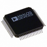
AD7606BSTZ Analog Devices Inc, AD7606BSTZ Datasheet - Page 7

AD7606BSTZ
Manufacturer Part Number
AD7606BSTZ
Description
IC DAS W/ADC 16BIT 8CH 64LQFP
Manufacturer
Analog Devices Inc
Type
Data Acquisition System (DAS), ADCr
Datasheet
1.AD7606BSTZ-6.pdf
(36 pages)
Specifications of AD7606BSTZ
Resolution (bits)
16 b
Data Interface
DSP, MICROWIRE™, Parallel, QSPI™, Serial, SPI™
Design Resources
Layout Considerations for an Expandable Multichannel Simultaneous Sampling Data Acquisition System Based on AD7606 (CN0148)
Sampling Rate (per Second)
200k
Voltage Supply Source
Single Supply
Voltage - Supply
4.75 V ~ 5.25 V
Operating Temperature
-40°C ~ 85°C
Mounting Type
Surface Mount
Package / Case
64-LFQFP
Sampling Rate
200kSPS
Input Channel Type
Single Ended
Supply Voltage Range - Analog
4.75V To 5.25V
Lead Free Status / RoHS Status
Lead free / RoHS Compliant
Available stocks
Company
Part Number
Manufacturer
Quantity
Price
Company:
Part Number:
AD7606BSTZ
Manufacturer:
ADI
Quantity:
1 000
Company:
Part Number:
AD7606BSTZ
Manufacturer:
Analog Devices Inc
Quantity:
135
Company:
Part Number:
AD7606BSTZ
Manufacturer:
Analog Devices Inc
Quantity:
10 000
Part Number:
AD7606BSTZ
Manufacturer:
ADI/亚德诺
Quantity:
20 000
Company:
Part Number:
AD7606BSTZ-4
Manufacturer:
ADI
Quantity:
1 000
Company:
Part Number:
AD7606BSTZ-4
Manufacturer:
Analog Devices Inc
Quantity:
135
Company:
Part Number:
AD7606BSTZ-4
Manufacturer:
Analog Devices Inc
Quantity:
10 000
Part Number:
AD7606BSTZ-4
Manufacturer:
ADI原装
Quantity:
20 000
Company:
Part Number:
AD7606BSTZ-4RL
Manufacturer:
Analog Devices Inc
Quantity:
10 000
Part Number:
AD7606BSTZ-4RL
Manufacturer:
ADI/亚德诺
Quantity:
20 000
Company:
Part Number:
AD7606BSTZ-6
Manufacturer:
Analog Devices Inc
Quantity:
10 000
TIMING SPECIFICATIONS
AV
Table 3.
Parameter
PARALLEL/SERIAL/BYTE MODE
PARALLEL/BYTE READ
t
t
OPERATION
t
t
t
t
t
t
t
t
t
t
t
t
t
t
t
t
t
CC
OS_SETUP
OS_HOLD
CYCLE
CONV
WAKE-UP STANDBY
WAKE-UP SHUTDOWN
RESET
1
2
3
4
5
6
7
8
9
10
11
12
3
Internal Reference
External Reference
= 4.75 V to 5.25 V, V
2
DRIVE
= 2.3 V to 5.25 V, V
Min
3.45
7.87
16.05
33
66
133
257
50
20
20
25
25
0
25
0
0
16
21
25
32
15
22
Limit at T
Typ
5
4
3
2
MIN
REF
, T
MAX
Max
5
9.7
4.15
9.1
18.8
39
78
158
315
100
30
13
40
0.5
25
= 2.5 V external reference/internal reference, T
Unit
μs
μs
μs
μs
μs
μs
μs
μs
μs
μs
μs
μs
μs
ms
ms
ns
ns
ns
ns
ns
ns
ns
ms
ns
ns
ns
ns
ns
ns
ns
ns
ns
ns
Rev. A | Page 7 of 36
1/throughput rate
Parallel mode, reading during or after conversion; or serial mode: V
4.75 V to 5.25 V, reading during a conversion using D
Serial mode reading during conversion; V
Serial mode reading after a conversion; V
Conversion time
Oversampling by 32; AD7606
Oversampling by 64; AD7606
STBY rising edge to CONVST x rising edge; power-up time from
standby mode
STBY rising edge to CONVST x rising edge; power-up time from
shutdown mode
STBY rising edge to CONVST x rising edge; power-up time from
shutdown mode
BUSY to OS x pin setup time
BUSY to OS x pin hold time
CONVST x high to BUSY high
Minimum CONVST x low pulse
Minimum CONVST x high pulse
BUSY falling edge to CS falling edge setup time
Maximum delay allowed between CONVST A, CONVST B rising edges
Minimum delay between RESET low to CONVST x high
CS to RD setup time
CS to RD hold time
RD low pulse width
V
V
V
V
RD high pulse width
CS high pulse width (see
Description
Oversampling off; AD7606
Oversampling off; AD7606-6
Oversampling off; AD7606-4
Oversampling by 2; AD7606
Oversampling by 4; AD7606
Oversampling by 8; AD7606
Oversampling by 16; AD7606
RESET high pulse width
Maximum time between last CS rising edge and BUSY falling edge
DRIVE
DRIVE
DRIVE
DRIVE
above 4.75 V
above 3.3 V
above 2.7 V
above 2.3 V
AD7606/AD7606-6/AD7606-4
Figure 5 CS and RD linked
A
= T
);
MIN
to T
DRIVE
DRIVE
MAX
= 2.3 V, D
= 3.3 V
, unless otherwise noted.
OUT
OUT
A and D
A and D
OUT
OUT
B lines
B lines
DRIVE
1
=


