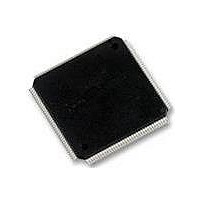
XR17D158IV-F Exar Corporation, XR17D158IV-F Datasheet - Page 23

XR17D158IV-F
Manufacturer Part Number
XR17D158IV-F
Description
IC UART PCI BUS OCTAL 144LQFP
Manufacturer
Exar Corporation
Type
IrDA or RS- 485r
Datasheet
1.XR17D158CV-F.pdf
(73 pages)
Specifications of XR17D158IV-F
Number Of Channels
8
Package / Case
144-LQFP
Features
*
Fifo's
64 Byte
Protocol
RS485
Voltage - Supply
3.3V, 5V
With Auto Flow Control
Yes
With Irda Encoder/decoder
Yes
With False Start Bit Detection
Yes
With Modem Control
Yes
Mounting Type
Surface Mount
Data Rate
6.25 Mbps
Supply Voltage (max)
5.5 V
Supply Voltage (min)
4.5 V
Supply Current
5 mA
Maximum Operating Temperature
+ 85 C
Minimum Operating Temperature
- 40 C
Mounting Style
SMD/SMT
Operating Supply Voltage
5 V
No. Of Channels
8
Uart Features
Tx/Rx FIFO Counters
Supply Voltage Range
3V To 5.5V
Operating Temperature Range
-40°C To +85°C
Digital Ic Case Style
LQFP
Rohs Compliant
Yes
Lead Free Status / RoHS Status
Lead free / RoHS Compliant
Lead Free Status / RoHS Status
Lead free / RoHS Compliant, Lead free / RoHS Compliant
Other names
1016-1292
Available stocks
Company
Part Number
Manufacturer
Quantity
Price
Company:
Part Number:
XR17D158IV-F
Manufacturer:
EXAR21
Quantity:
100
Company:
Part Number:
XR17D158IV-F
Manufacturer:
Exar Corporation
Quantity:
10 000
Part Number:
XR17D158IV-F
Manufacturer:
EXAR/艾科嘉
Quantity:
20 000
xr
REV. 1.2.2
DVID [15:8]
Device identification for the type of UART. The upper nibble indicates it is a XR17Dxxx series with lower nibble
indicating the number of channels.
Examples:
XR17C158 or XR17D158 = 0x28
XR17C154 or XR17D154 = 0x24
XR17C152 or XR17D152 = 0x22
DREV [7:0]
Revision number of the XR17D158. A 0x01 represents "revision-A" with 0x02 for rev-B and so forth.
REGB [23:16] (default 0x00)
REGB register provides a control for simultaneous write to all 8 UARTs configuration register or individually.
This is very useful for device initialization in the power up and reset routines. Also, the register provides a
facility to interface to the non-volatile memory device such as a 93C46 EEPROM. In embedded applications,
the user can use this facility to store proprietary data.
The D158 provides 8 multi-purpose inputs/outputs [MPIO7:0] for general use. Each pin can be programmed to
be an input or output function. The input logic state can be set for normal or inverted level, and optionally set to
generate an interrupt. The outputs can be set to be normal logic 1 or 0 state, or 3-state. Their functions and
definitions are programmed through 5 registers: MPIOINT, MPIOLVL, MPIO3T, MPIOINV and MPIOSEL. If all
8 pins are set for inputs, all 8 interrupts would be OR’ed together. The OR’ed interrupt is reported in the
channel 0 UART interrupt status, see Interrupt Status Register. The pins may also be programmed to be
outputs and to the 3-state condition for signal sharing.
Bit 7 represents MPIO7 pin and bit 0 represents MPIO0 pin. There are 5 registers that select, control and
monitor the 8 multipurpose inputs and outputs.
REGB[16](Read/Write)
REGB[19:17]
REGB[20] (Write-Only)
REGB[21] (Write-Only)
REGB[22] (Write-Only)
REGB[23] (Read-Only)
2.2.8
2.2.9
2.2.10
REGB Register
Multi-Purpose Inputs and Outputs
MPIO REGISTER
Logic 0 (default) write to each UART configuration registers individually.
Logic 1 enables simultaneous write to all 8 UARTs configuration register.
Reserved
Control the EECK, clock, output (pin 116) on the EEPROM interface.
Control the EECS, chips select, output (pin 115) to the EEPROM device.
EEDI (pin 114) data input. Write data to the EEPROM device.
EEDO (pin 113) data output. Read data from the EEPROM device.
Figure 8
23
UNIVERSAL (3.3V AND 5V) PCI BUS OCTAL UART
shows the internal circuitry.
XR17D158


