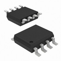
FOD2712A Fairchild Optoelectronics Group, FOD2712A Datasheet

FOD2712A
Specifications of FOD2712A
Available stocks
Related parts for FOD2712A
FOD2712A Summary of contents
Page 1
... It is primarily intended for use as the error amplifier/ reference voltage/optocoupler function in isolated power supplies and dc/dc converters. When using the FOD2712A, power supply designers can reduce the component count and save space in tightly packaged designs. The tight tolerance reference elimi- nates the need for adjustments in many applications. ...
Page 2
... Typical Application FAN4803 PWM V 1 Control ©2010 Fairchild Semiconductor Corporation FOD2712A Rev. 1.0.1 Functional Description Not connected Phototransistor Collector Phototransistor Emitter Not connected Ground Error Amplifier Compensation. This pin is the output of the error amplifier.* Voltage Feedback. This pin is the inverting input to the error amplifi ...
Page 3
... PD3 Total Power Dissipation Notes: 1. Derate linearly from 25° rate of 2.42mW/°C 2. Derate linearly from 25° rate of 1.42mW/°C. 3. Derate linearly from 25° rate of 2.42mW/°C. ©2010 Fairchild Semiconductor Corporation FOD2712A Rev. 1.0 25°C unless otherwise specified) A Parameter -40 to +125 (1) ...
Page 4
... The dynamic impedance is defined as |Z resistors (see Figure 2), the total dynamic impedance of the circuit is given by: ∆V ≈ × ------- - Z 1 OUT, TOT ∆I OUT ©2010 Fairchild Semiconductor Corporation FOD2712A Rev. 1.0 12V 25°C unless otherwise specified Test Conditions I = 10mA, V LED (Fig. COMP FB (Fig ...
Page 5
... Vcm, to assure that the output will remain high. Common mode transient immunity at output low is the maximum tolerable (negative) dVcm/dt on the trailing edge of the common pulse signal,Vcm, to assure that the output will remain low. ©2010 Fairchild Semiconductor Corporation FOD2712A Rev. 1.0 12V 25°C unless otherwise specified) (Continued) ...
Page 6
... REF 5 Figure (min) Test Circuit REF F, LED I (LED REF Figure 3. I Test Circuit REF Figure 5. I Test Circuit CEO ©2010 Fairchild Semiconductor Corporation FOD2712A Rev. 1.0 Figure 2. ∆ CEO (LED COMP R2 V REF 5 ∆V Test Circuit REF/ COMP I (OFF (LED) ...
Page 7
... Test Circuits (Continued + OUT 2.2kΩ V OUT ©2010 Fairchild Semiconductor Corporation FOD2712A Rev. 1.0 0 Figure 7. Frequency Response Test Circuit VCM _ + 10V P-P Figure 8. CMH and CML Test Circuit 7 47Ω 1µ 0.47V = www.fairchildsemi.com ...
Page 8
... CATHODE VOLTAGE (V) COMP Fig. 10 Reference Voltage vs. Ambient Temperature 1.254 I = 10mA LED 1.248 1.242 1.236 1.230 -40 - – AMBIENT TEMPERATURE (°C) A ©2010 Fairchild Semiconductor Corporation FOD2712A Rev. 1.0.1 Fig. 9b LED Current vs. Cathode Voltage 150 T 120 A V COMP -30 -60 -90 -120 -150 -1.0 0.5 1 ...
Page 9
... V – FORWARD VOLTAGE (V) F Fig. 15 Collector Current vs. Ambient Temperature -40 - – AMBIENT TEMPERATURE (°C) A ©2010 Fairchild Semiconductor Corporation FOD2712A Rev. 1.0.1 (Continued) 1000 V CE 100 10 0°C 1 0.1 1.20 1.25 1.30 1.35 -40 Fig. 16 Current Transfer Ratio vs. LED Current 160 140 I = 20mA ...
Page 10
... Typical Performance Curves Fig. 18 Collector Current vs. Collector Voltage 25° – COLLECTOR-EMITTER VOLTAGE (V) CE -10 -15 ©2010 Fairchild Semiconductor Corporation FOD2712A Rev. 1.0.1 (Continued) Fig. 19 Delta LED LED - LED LED - -40 Fig. 20 Voltage Gain vs. Frequency 0 500Ω =1kΩ 100 FREQUENCY kHz 10 /Delta V vs. Ambient Temperature ...
Page 11
... Feedback Output voltage of a converter is determined by selecting a resistor divider from the regulated output to the FB pin. The FOD2712A attempts to regulate its FB pin to the ref- erence voltage, 1.24V. The ratio of the two resistors should thus be ...
Page 12
... Package specifications do not expand the terms of Fairchild’s worldwide terms and conditions, specifically the warranty therein, which covers Fairchild products. Always visit Fairchild Semiconductor’s online packaging area for the most recent package drawings: http://www.fairchildsemi.com/packaging/ ©2010 Fairchild Semiconductor Corporation FOD2712A Rev. 1.0.1 8 0.164 (4.16) 0.144 (3.66) 1 ...
Page 13
... FOD2712AV R2 FOD2712AR2 R2V FOD2712AR2V Marking Information Definitions ©2010 Fairchild Semiconductor Corporation FOD2712A Rev. 1.0.1 VDE 0884 Tape and reel (2500 units per reel) VDE 0884, Tape and reel (2500 units per reel) 1 2712A Fairchild logo Device number VDE mark (Note: Only appears on parts ordered with VDE option – ...
Page 14
... Carrier Tape Specifications 3.50 ± 0.20 0.30 MAX 8.3 ± 0.10 0.1 MAX User Direction of Feed Dimensions in mm ©2010 Fairchild Semiconductor Corporation FOD2712A Rev. 1.0.1 8.0 ± 0.10 2.0 ± 0.05 4.0 ± 0.10 6.40 ± 0.20 14 Ø1.5 MIN 1.75 ± 0.10 5.5 ± ...
Page 15
... Time (t ) Maintained Above (T L Peak Body Package Temperature Time (t ) within 5°C of 260°C P Ramp-down Rate (T Time 25°C to Peak Temperature ©2010 Fairchild Semiconductor Corporation FOD2712A Rev. 1.0.1 Max. Ramp-up Rate = 3°C/S Max. Ramp-down Rate = 6°C/S Tsmax Preheat Area Tsmin t s 120 240 Time 25° ...
Page 16
... Datasheet Identification Product Status Advance Information Formative / In Design Preliminary First Production No Identification Needed Full Production Obsolete Not In Production ©2010 Fairchild Semiconductor Corporation FOD2712A Rev. 1.0.1 ® PowerTrench PowerXS™ SM Programmable Active Droop™ ® QFET QS™ Quiet Series™ RapidConfigure™ ...


