13192EVK-SFTE Freescale Semiconductor, 13192EVK-SFTE Datasheet - Page 15
13192EVK-SFTE
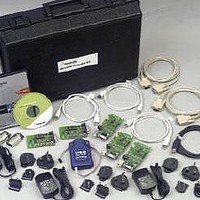
Manufacturer Part Number
13192EVK-SFTE
Description
EVAL KIT HARDWARE DEV
Manufacturer
Freescale Semiconductor
Type
802.15.4/Zigbeer
Specifications of 13192EVK-SFTE
Contents
Hardware, Software, Documentation and CodeWarrior™ Standard Edition
Wireless Frequency
2.4 GHz
Interface Type
SPI
Modulation
DSSS OQPSK
Security
128 bit AES
For Use With/related Products
MC13193
Lead Free Status / RoHS Status
Lead free / RoHS Compliant


Freescale Semiconductor
1
2
3
The transceiver GPIO pins default to inputs at reset. There are no programmable pullups on these pins. Unused GPIO pins
should be tied to ground if left as inputs, or if left unconnected, they should be programmed as outputs set to the low state.
During low power modes, input must remain driven by MCU.
By default MISO is tri-stated when CE is negated. For low power operation, miso_hiz_en (Bit 11, Register 07) should be set
to zero so that MISO is driven low when CE is negated.
Pin #
EP
20
21
22
23
24
25
26
27
28
29
30
31
32
IRQ
VDDD
VDDINT
GPIO5
GPIO6
GPIO7
XTAL1
XTAL2
VDDLO2
VDDLO1
VDDVCO
VBATT
VDDA
Ground
Pin Name
1
1
1
Digital Output
Power Output
Power Input
Digital Input/Output
Digital Input/Output
Digital Input/Output
Input
Input/Output
Power Input
Power Input
Power Output
Power Input
Power Output
Type
Table 8. Pin Function Description (continued)
MC13192 Technical Data, Rev. 3.3
Active Low Interrupt Request.
Digital regulated supply bypass.
Digital interface supply & digital regulator input.
Connect to Battery.
General Purpose Input/Output 5.
General Purpose Input/Output 6.
General Purpose Input/Output 7.
Crystal Reference oscillator input.
Crystal Reference oscillator output
Note: Do not load this pin by using it as a 16 MHz
LO2 VDD supply. Connect to VDDA externally.
LO1 VDD supply. Connect to VDDA externally.
VCO regulated supply bypass.
Analog voltage regulators Input. Connect to Battery.
Analog regulated supply Output. Connect to directly
VDDLO1 and VDDLO2 externally and to PAO±
through a frequency trap.
Note: Do not use this pin to supply circuitry external to
the chip.
External paddle / flag ground.
source. Measure 16 MHz output at Pin 15,
CLKO, programmed for 16 MHz. See the
MC13192 Reference Manual for details.
Description
Open drain device.
Programmable 40
k
Interrupt can be
serviced every 6 µs
with <20 pF load.
Optional external
pull-up must be >4
k
Decouple to ground.
2.0 to 3.4 V.
Decouple to ground.
See Footnote 1
See Footnote 1
See Footnote 1
Connect to 16 MHz
crystal and load
capacitor.
Connect to 16 MHz
crystal and load
capacitor.
Decouple to ground.
Decouple to ground.
Decouple to ground.
Connect to ground.
Ω
Ω
.
internal pull-up.
Functionality
Pin Connections
15
Related parts for 13192EVK-SFTE
Image
Part Number
Description
Manufacturer
Datasheet
Request
R

Part Number:
Description:
EVAL KIT HARDWARE DEV
Manufacturer:
Freescale Semiconductor
Datasheet:

Part Number:
Description:
Manufacturer:
Freescale Semiconductor, Inc
Datasheet:
Part Number:
Description:
Manufacturer:
Freescale Semiconductor, Inc
Datasheet:
Part Number:
Description:
Manufacturer:
Freescale Semiconductor, Inc
Datasheet:
Part Number:
Description:
Manufacturer:
Freescale Semiconductor, Inc
Datasheet:
Part Number:
Description:
Manufacturer:
Freescale Semiconductor, Inc
Datasheet:
Part Number:
Description:
Manufacturer:
Freescale Semiconductor, Inc
Datasheet:
Part Number:
Description:
Manufacturer:
Freescale Semiconductor, Inc
Datasheet:
Part Number:
Description:
Manufacturer:
Freescale Semiconductor, Inc
Datasheet:
Part Number:
Description:
Manufacturer:
Freescale Semiconductor, Inc
Datasheet:
Part Number:
Description:
Manufacturer:
Freescale Semiconductor, Inc
Datasheet:
Part Number:
Description:
Manufacturer:
Freescale Semiconductor, Inc
Datasheet:
Part Number:
Description:
Manufacturer:
Freescale Semiconductor, Inc
Datasheet:
Part Number:
Description:
Manufacturer:
Freescale Semiconductor, Inc
Datasheet:
Part Number:
Description:
Manufacturer:
Freescale Semiconductor, Inc
Datasheet: