13192EVB-BDM-A0E Freescale Semiconductor, 13192EVB-BDM-A0E Datasheet - Page 17
13192EVB-BDM-A0E
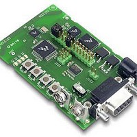
Manufacturer Part Number
13192EVB-BDM-A0E
Description
EVAL BOARD HARDWARE DEV
Manufacturer
Freescale Semiconductor
Type
802.15.4/Zigbeer
Specifications of 13192EVB-BDM-A0E
Contents
Hardware, Software, Documentation and USB Multilink
Wireless Frequency
2.4 GHz
Interface Type
SPI
Modulation
DSSS OQPSK
Security
128 bit AES
Operating Voltage
2 VDC to 3.4 VDC
Output Power
1 mW
Operating Temperature Range
- 40 C to + 85 C
For Use With/related Products
MC13193
Lead Free Status / RoHS Status
Lead free / RoHS Compliant


8
This section provides application specific information regarding crystal oscillator reference frequency, a
basic design example for interfacing the MC13192 to an MCU and recommended crystal usage.
8.1
The 802.15.4 Standard requires that several frequency tolerances be kept within ± 40 ppm accuracy. This
means that a total offset up to 80 ppm between transmitter and receiver will still result in acceptable
performance. The MC13192 transceiver provides onboard crystal trim capacitors to assist in meeting this
performance.
The primary determining factor in meeting this specification is the tolerance of the crystal oscillator
reference frequency. A number of factors can contribute to this tolerance and a crystal specification will
quantify each of them:
Freescale requires the use of a 16 MHz crystal with a <9 pF load capacitance. The MC13192 does not
contain a reference divider, so 16 MHz is the only frequency that can be used. A crystal requiring higher
load capacitance is prohibited because a higher load on the amplifier circuit may compromise its
performance. The crystal manufacturer defines the load capacitance as that total external capacitance seen
across the two terminals of the crystal. The oscillator amplifier configuration used in the MC13192
requires two balanced load capacitors from each terminal of the crystal to ground. As such, the capacitors
are seen to be in series by the crystal, so each must be <18 pF for proper loading.
In the reference schematic, the external load capacitors are shown as 6.8 pF each, used in conjunction with
a crystal that requires an 8 pF load capacitance. The default internal trim capacitor value (2.4 pF) and stray
capacitance total value (6.8 pF) sum up to 9.2 pF giving a total of 16 pF. The value for the stray capacitance
was determined empirically assuming the default internal trim capacitor value and for a specific board
layout. A different board layout may require a different external load capacitor value. The on-chip trim
capability may be used to determine the closest standard value by adjusting the trim value via the SPI and
observing the frequency at CLKO. Each internal trim load capacitor has a trim range of approximately
5 pF in 20 fF steps.
Initial tolerance for the internal trim capacitance is approximately ±15%.
Freescale Semiconductor
1. The initial (or make) tolerance of the crystal resonant frequency itself.
2. The variation of the crystal resonant frequency with temperature.
3. The variation of the crystal resonant frequency with time, also commonly known as aging.
4. The variation of the crystal resonant frequency with load capacitance, also commonly known as
Applications Information
pulling. This is affected by:
a) The external load capacitor values - initial tolerance and variation with temperature.
b) The internal trim capacitor values - initial tolerance and variation with temperature.
c) Stray capacitance on the crystal pin nodes - including stray on-chip capacitance, stray package
Crystal Oscillator Reference Frequency
capacitance and stray board capacitance; and its initial tolerance and variation with
temperature.
MC13192 Technical Data, Rev. 3.3
Applications Information
17
Related parts for 13192EVB-BDM-A0E
Image
Part Number
Description
Manufacturer
Datasheet
Request
R

Part Number:
Description:
EVAL BOARD HARDWARE DEV
Manufacturer:
Freescale Semiconductor
Datasheet:

Part Number:
Description:
Manufacturer:
Freescale Semiconductor, Inc
Datasheet:
Part Number:
Description:
Manufacturer:
Freescale Semiconductor, Inc
Datasheet:
Part Number:
Description:
Manufacturer:
Freescale Semiconductor, Inc
Datasheet:
Part Number:
Description:
Manufacturer:
Freescale Semiconductor, Inc
Datasheet:
Part Number:
Description:
Manufacturer:
Freescale Semiconductor, Inc
Datasheet:
Part Number:
Description:
Manufacturer:
Freescale Semiconductor, Inc
Datasheet:
Part Number:
Description:
Manufacturer:
Freescale Semiconductor, Inc
Datasheet:
Part Number:
Description:
Manufacturer:
Freescale Semiconductor, Inc
Datasheet:
Part Number:
Description:
Manufacturer:
Freescale Semiconductor, Inc
Datasheet:
Part Number:
Description:
Manufacturer:
Freescale Semiconductor, Inc
Datasheet:
Part Number:
Description:
Manufacturer:
Freescale Semiconductor, Inc
Datasheet:
Part Number:
Description:
Manufacturer:
Freescale Semiconductor, Inc
Datasheet:
Part Number:
Description:
Manufacturer:
Freescale Semiconductor, Inc
Datasheet:
Part Number:
Description:
Manufacturer:
Freescale Semiconductor, Inc
Datasheet: