MW7IC2240NBR1 Freescale Semiconductor, MW7IC2240NBR1 Datasheet - Page 4
MW7IC2240NBR1
Manufacturer Part Number
MW7IC2240NBR1
Description
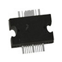
IC PWR AMP RF 4W TO-272-16
Manufacturer
Freescale Semiconductor
Specifications of MW7IC2240NBR1
Current - Supply
420mA
Frequency
2.11GHz ~ 2.17GHz
Gain
30dB
P1db
40W
Package / Case
TO-272-16
Rf Type
W-CDMA
Test Frequency
2.14GHz
Voltage - Supply
32V
Channel Type
N
Drain Source Voltage (max)
65V
Output Power (max)
4W
Power Gain (typ)@vds
28dB
Frequency (min)
2GHz
Frequency (max)
2.2GHz
Package Type
TO-272 WB EP
Pin Count
16
Operating Temp Range
-65C to 225C
Mounting
Surface Mount
Mode Of Operation
1-Carrier W-CDMA
Number Of Elements
1
Screening Level
Military
Lead Free Status / RoHS Status
Lead free / RoHS Compliant
Noise Figure
-
Lead Free Status / Rohs Status
Compliant
Available stocks
Company
Part Number
Manufacturer
Quantity
Price
Company:

Part Number:
MW7IC2240NBR1
Manufacturer:
FREESCALE
Quantity:
1 400
Part Number:
MW7IC2240NBR1
Manufacturer:
FREESCALE
Quantity:
20 000


MW7IC2040NR1 MW7IC2040GNR1 MW7IC2040NBR1
4
Table 5. Electrical Characteristics
Typical W - CDMA Performance — 1800 MHz (In Freescale W - CDMA 1805 - 1880 MHz Test Fixture, 50 ohm system) V
I
Input Signal PAR = 7.5 dB @ 0.01% Probability on CCDF. ACPR measured in 3.84 MHz Channel Bandwidth @ ±5 MHz Offset.
Typical GSM EDGE Performance — 1800 MHz (In Freescale GSM EDGE 1805 - 1880 MHz Test Fixture, 50 ohm system) V
P
Typical GSM EDGE Performance — 1900 MHz (In Freescale GSM EDGE 1930 - 1990 MHz Test Fixture, 50 ohm system) V
P
Typical CW Performance (In Freescale GSM EDGE 1930 - 1990 MHz Test Fixture, 50 ohm system) V
I
DQ1
DQ2
out
out
Power Gain
Power Added Efficiency
Adjacent Channel Power Ratio
Input Return Loss
Power Gain
Power Added Efficiency
Error Vector Magnitude
Spectral Regrowth at 400 kHz Offset
Spectral Regrowth at 600 kHz Offset
Power Gain
Power Added Efficiency
Error Vector Magnitude
Spectral Regrowth at 400 kHz Offset
Spectral Regrowth at 600 kHz Offset
Power Gain
Power Added Efficiency
Input Return Loss
P
out
= 16 W Avg., I
= 16 W Avg., I
= 130 mA, I
= 430 mA, P
@ 1 dB Compression Point
DQ2
out
DQ1
DQ1
= 40 W CW, 1805 - 1880 MHz and 1930 - 1990 MHz
= 330 mA, P
= 90 mA, I
= 90 mA, I
Characteristic
out
DQ2
DQ2
= 4 W Avg., 1805 - 1880 MHz, Single - Carrier W - CDMA, 3GPP Test Model 1, 64 DPCH, 45.2% Clipping,
= 430 mA, 1805 - 1880 MHz EDGE Modulation
= 430 mA, 1930 - 1990 MHz EDGE Modulation
(T
C
= 25°C unless otherwise noted) (continued)
Symbol
ACPR
P1dB
EVM
EVM
PAE
PAE
SR1
SR2
PAE
SR1
SR2
PAE
G
G
G
G
IRL
IRL
ps
ps
ps
ps
Min
—
—
—
—
—
—
—
—
—
—
—
—
—
—
—
—
—
—
DD
= 28 Vdc, I
33.5
16.5
Typ
- 50
- 62
- 77
- 62
- 80
- 15
1.5
1.5
33
35
30
33
31
50
45
- 6
Freescale Semiconductor
DQ1
Max
DD
—
—
—
—
—
—
—
—
—
—
—
—
—
—
—
—
—
—
= 90 mA,
RF Device Data
= 28 Vdc,
DD
DD
= 28 Vdc,
= 28 Vdc,
% rms
% rms
Unit
dBc
dBc
dBc
dBc
dBc
dB
dB
dB
dB
dB
dB
%
%
%
%
W
Related parts for MW7IC2240NBR1
Image
Part Number
Description
Manufacturer
Datasheet
Request
R

Part Number:
Description:
Manufacturer:
Freescale Semiconductor, Inc
Datasheet:
Part Number:
Description:
Manufacturer:
Freescale Semiconductor, Inc
Datasheet:
Part Number:
Description:
Manufacturer:
Freescale Semiconductor, Inc
Datasheet:
Part Number:
Description:
Manufacturer:
Freescale Semiconductor, Inc
Datasheet:
Part Number:
Description:
Manufacturer:
Freescale Semiconductor, Inc
Datasheet:
Part Number:
Description:
Manufacturer:
Freescale Semiconductor, Inc
Datasheet:
Part Number:
Description:
Manufacturer:
Freescale Semiconductor, Inc
Datasheet:
Part Number:
Description:
Manufacturer:
Freescale Semiconductor, Inc
Datasheet:
Part Number:
Description:
Manufacturer:
Freescale Semiconductor, Inc
Datasheet:
Part Number:
Description:
Manufacturer:
Freescale Semiconductor, Inc
Datasheet:
Part Number:
Description:
Manufacturer:
Freescale Semiconductor, Inc
Datasheet:
Part Number:
Description:
Manufacturer:
Freescale Semiconductor, Inc
Datasheet:
Part Number:
Description:
Manufacturer:
Freescale Semiconductor, Inc
Datasheet:
Part Number:
Description:
Manufacturer:
Freescale Semiconductor, Inc
Datasheet:
Part Number:
Description:
Manufacturer:
Freescale Semiconductor, Inc
Datasheet: