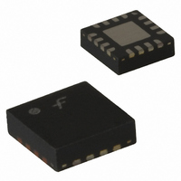
RMPA2453 Fairchild Semiconductor, RMPA2453 Datasheet

RMPA2453
Specifications of RMPA2453
Available stocks
Related parts for RMPA2453
RMPA2453 Summary of contents
Page 1
... RMPA2453 2.4–2.5 GHz InGaP HBT Linear Power Amplifier General Description The RMPA2453 power amplifier is designed for high performance WLAN applications in the 2.4–2.5 GHz frequency band. The low profile 16 pin 0.9 mm package with internal matching on both input and output to 50 Ω minimizes next level PCB space and allows for simplified integration ...
Page 2
... GHz 3.0 3.3 3 133 160 mA 145 165 mA 3 2.5 3 3.5 4.5 % 515 600 mV 5.0 7.0 dBm 21.0 dBm Min Typ Max Units 2.4 2.5 GHz 3.0 3.3 3 250 mA -35 dBc -55 dBc 24.0 dBm RMPA2453 Rev. D ...
Page 3
... P1dB. OUT Min Typ Max Units 2.4 2.5 GHz 3.0 3.3 3 105 135 mA 10.0 12.5 15 26.5 dBm 0.7 mA <1.0 µ 2.0 V 7.0 9.0 dBm -45 dBc -42 dBc 2.0 2.4 V 0.0 0.8 V 150 µA <1 µS <1 µS -65 dBc RMPA2453 Rev. D ...
Page 4
... Total Integrated Output Channel Power 54Mbps Data Rate OFDM 16.7MHz Total Integrated Output Power (dBm) 54Mbps Data Rate OFDM 16.7MHz Total Integrated Output Power (dBm) 54Mbps Data Rate OFDM 16.7MHz Total Integrated Output Power (dBm) RMPA2453 Rev ...
Page 5
... Data Rate OFDM 16.7MHz Total Integrated Output Power (dBm) 54Mbps Data Rate OFDM 16.7MHz Vm12=3.3V, Vc1=3.3V, Vc2=3. Total Integrated Output Power (dBm) 54Mbps Data Rate OFDM 16.7MHz Vm12=3.3V, Vc1=3.3V, Vc2=3. Total Integrated Output Power (dBm) RMPA2453 Rev ...
Page 6
... Typical Characteristics Spec ANA Pout = 23 dBm Pin adjusted to the point where the part just begins to approach the 802.11b spectral mask requirements. RMPA2453 Spectral Plot Showing Compliance to 802.11b Spectral Mask Requirements @ 23 dBm Modulated Output Power Single Tone Typical Small Signal S-parameters versus Frequency Vm12=3 ...
Page 7
... Front Side View Bottom View as Viewed from Bottom Note: Dimensions do not include protrusions or mold flash. These are not to exceed 0.006" (.155mm) on any side. Evaluation Board Schematic ©2004 Fairchild Semiconductor Corporation See Detail A Detail A 2453 WWWY Backside Ground 2453 WWWY RMPA2453 Rev. D ...
Page 8
... Evaluation Board of Materials Evaluation Board Layout ©2004 Fairchild Semiconductor Corporation Actual Board Size = 2.0" X 1.5" RMPA2453 Rev. D ...
Page 9
... Shut down current flow into the pins: Pin Current VM12 <0.7 mA VC1 <1 nA VC2 < <0. Recommended turn-off sequence: Use reverse order described in the turn-on sequence above. Note: 1: Turn on sequence is not critical and it is not necessary to sequence power supplies in actual system level design. on pin VREG from +0. RMPA2453 Rev. D ...
Page 10
... TRADEMARKS The following are registered and unregistered trademarks Fairchild Semiconductor owns or is authorized to use and is not intended exhaustive list of all such trademarks. ACEx™ FAST ActiveArray™ FASTr™ Bottomless™ FPS™ CoolFET™ FRFET™ CROSSVOLT™ GlobalOptoisolator™ ...


