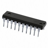
TDA9801/V1,112 NXP Semiconductors, TDA9801/V1,112 Datasheet - Page 9

TDA9801/V1,112
Manufacturer Part Number
TDA9801/V1,112
Description
IC PLL DEMODULATOR 20-DIP
Manufacturer
NXP Semiconductors
Datasheet
1.TDA9801V1112.pdf
(32 pages)
Specifications of TDA9801/V1,112
Package / Case
20-DIP (0.300", 7.62mm)
Function
Demodulator, Detector
Current - Supply
70mA
Voltage - Supply
4.5 V ~ 9.9 V
Mounting Style
Through Hole
Lead Free Status / RoHS Status
Lead free / RoHS Compliant
Gain
-
Noise Figure
-
P1db
-
Lo Frequency
-
Rf Frequency
-
Lead Free Status / RoHS Status
Lead free / RoHS Compliant, Lead free / RoHS Compliant
Other names
935260644112
TDA9801N
TDA9801N
TDA9801N
TDA9801N
Philips Semiconductors
1999 Aug 26
I
I
B
PSRR
Buffer amplifier and noise clipper input: pin VI
R
C
V
Buffer amplifier output: pin CVBS
G
B
V
V
V
V
R
I
I
I
Measurements from VIF inputs to CVBS output (330
V
G
B
o(sink)(max)
o(source)(max)
bias
o(sink)(max)
o(source)(max)
V
V
dif
v( 3dB)
H(sup)
I
v( 3dB)
o(v)(p-p)
v(clu)
v(cll)
sync
o(CVBS)(p-p)
v( 3dB)
i
i
o
Single standard VIF-PLL demodulator
and FM-PLL detector
v
dif
o(CVBS)
o(bl)
SYMBOL
VSO
maximum AC and DC
output sink current
maximum AC and DC
output source current
harmonics suppression in
video signal
power supply ripple
rejection at pin VSO
input resistance
input capacitance
DC input voltage
voltage gain
video output voltage
(peak-to-peak value)
upper video clipping
voltage level
lower video clipping voltage
level
sync pulse voltage level
output resistance
DC bias current
maximum AC and DC
output sink current
maximum AC and DC
output source current
CVBS output voltage
(peak-to-peak value)
deviation of CVBS output
voltage
black level tilt
differential gain
differential phase
3 dB video bandwidth
3 dB video bandwidth
3 dB video bandwidth
PARAMETER
C
C
note 10
see Fig.7
pin VI not connected
note 11
C
sound carrier off;
see Fig.12
internal emitter-follower at
pin CVBS
V
V
at B/G standard
gain variation; note 12
“CCIR, line 330” or
“NTC-7 Composite”
“CCIR, line 330” or
“NTC-7 Composite”
C
P
P
L
L
L
L
50 dB gain control
30 dB gain control
< 50 pF; R
< 50 pF; R
< 20 pF; R
< 20 pF; R
= 5 V
= 9 V
CONDITIONS
9
connected between pins VSO and VI, sound carrier off)
L
L
L
L
> 1 k
> 1 k ;
> 1 k
> 1 k
1.4
2.0
7
35
32
2.6
1.4
1.5
6
8
1.7
3.9
1.8
1.4
2.4
1.7
1.8
6
MIN.
10
40
35
3.3
2
1.8
7
11
2.0
4.0
1.0
1.35
2.5
2.0
2.2
2
2
8
TYP.
4.0
3.0
2.1
7.5
2.3
1.1
10
2.3
2.6
0.5
0.1
1
5
4
Product specification
MAX.
TDA9801
mA
mA
MHz
dB
dB
k
pF
V
dB
MHz
V
V
V
V
mA
mA
mA
V
V
dB
dB
%
%
deg
MHz
UNIT


