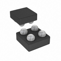
ADL5500ACBZ-P7 Analog Devices Inc, ADL5500ACBZ-P7 Datasheet

ADL5500ACBZ-P7
Specifications of ADL5500ACBZ-P7
ADL5500ACBZ-P7TR
Available stocks
Related parts for ADL5500ACBZ-P7
ADL5500ACBZ-P7 Summary of contents
Page 1
FEATURES True rms response Excellent temperature stability ±0.1 dB accuracy vs. temperature over top input range input dynamic range at 3.9 GHz 50 Ω input impedance 1250 mV rms, +15 dBm, maximum input ...
Page 2
ADL5500 TABLE OF CONTENTS Features .............................................................................................. 1 Applications....................................................................................... 1 General Description ......................................................................... 1 Functional Block Diagram .............................................................. 1 Revision History ............................................................................... 2 Specifications..................................................................................... 3 Absolute Maximum Ratings............................................................ 7 ESD Caution.................................................................................. 7 Pin Configuration and Function Descriptions............................. 8 Typical Performance Characteristics ...
Page 3
SPECIFICATIONS T = 25° 3 nF, light condition ≤ 600 LUX, unless otherwise noted FLT Table 1. Parameter FREQUENCY RANGE RMS CONVERSION (f = 100 MHz) Input Impedance Input Return Loss 1 ...
Page 4
ADL5500 Parameter RMS CONVERSION (f = 900 MHz) Input Impedance Input Return Loss 1 Dynamic Range ±0.1 dB Error 2 3 ±0.25 dB Error 3 ±1 dB Error 3 ±2 dB Error Maximum Input Level Minimum Input Level Conversion Gain ...
Page 5
Parameter RMS CONVERSION (f = 2350 MHz) Input Impedance Input Return Loss 1 Dynamic Range ±0.1 dB Error 2 3 ±0.25 dB Error 3 ±1 dB Error 3 ±2 dB Error Maximum Input Level Minimum Input Level Conversion Gain 4 ...
Page 6
ADL5500 Parameter RMS CONVERSION (f = 3900 MHz) Input Impedance Input Return Loss 1 Dynamic Range ±0.1 dB Error 2 3 ±0.25 dB Error 3 ±1 dB Error 3 ±2 dB Error Maximum Input Level Minimum Input Level Conversion Gain ...
Page 7
ABSOLUTE MAXIMUM RATINGS Table 2. Parameter Rating Supply Voltage V 5 VRMS RFIN 1.25 V rms Equivalent Power Ω 15 dBm Internal Power Dissipation 150 mW θ (WLCSP) 260°C/W JA Maximum Junction Temperature ...
Page 8
ADL5500 PIN CONFIGURATION AND FUNCTION DESCRIPTIONS Table 3. Pin Function Descriptions Ball No. Mnemonic Description 1 VRMS Output Pin. Rail-to-rail voltage output with limited current drive capability. The output has an internal 1 kΩ series resistance. High resistive loads are ...
Page 9
TYPICAL PERFORMANCE CHARACTERISTICS T = 25° 5 nF, light condition ≤ 600 LUX, Colors: black = +25°C, blue = −40°C, red = +85°C, unless otherwise noted FLT 10 1 0.1 0.03 –25 ...
Page 10
ADL5500 –1 –2 –3 –25 –20 –15 –10 –5 INPUT (dBm) Figure 10. Temperature Drift Distributions for 55 Devices at −40°C, +25°C, and +85°C vs. +25°C Linear Reference, Frequency 450 MHz, Supply 5 ...
Page 11
INPUT (dBm) Figure 16. Output Delta from +25°C Output Voltage for 55 Devices at −40°C and +85°C, Frequency 450 MHz, Supply 5 ...
Page 12
ADL5500 10 CW QPSK, 4.8dB CF 8PSK, 4.8dB CF 16QAM, 6.3dB CF 64QAM, 7.4dB CF 1 0.1 0.03 –25 –20 –15 –10 –5 INPUT (dBm) Figure 22. Output vs. Input Level with Different Waveforms, 10 MHz Signal BW for All ...
Page 13
ADL5500 TEK P6204 1 VRMS VPOS 4 FET PROBE C4 2 COMM RFIN 3 TEK TDS784C SCOPE Figure 28. Hardware Configuration for Output Response to Modulated Pulse Input 400mV rms RF INPUT 250mV rms 160mV rms 70mV rms 400μs PER ...
Page 14
ADL5500 CIRCUIT DESCRIPTION The ADL5500 is an rms-responding (mean power) detector that provides an approach to the exact measurement of RF power that is independent of waveform. It achieves this function by using a proprietary technique in which the outputs ...
Page 15
APPLICATIONS BASIC CONNECTIONS Figure 33 shows the basic connections for the ADL5500. The device is powered by a single supply of between 2.7 V and 5.5 V with a quiescent current of 1.0 mA. The VPOS pin is decoupled using ...
Page 16
ADL5500 INPUT COUPLING USING A SERIES RESISTOR Figure 36 shows a technique for coupling the input signal into the ADL5500 that can be applicable where the input signal is much larger than the input range of the ADL5500. A series ...
Page 17
OUTPUT DRIVE CAPABILITY AND BUFFERING The ADL5500 is capable of sourcing an output current of approximately 3 mA. The output current is sourced through the on-chip 1 kΩ series resistor; therefore, any load resistor forms a voltage divider with this ...
Page 18
ADL5500 DEVICE CALIBRATION AND ERROR CALCULATION Because slope and intercept vary from device to device, board- level calibration must be performed to achieve high accuracy. In general, calibration is performed by applying two input power levels to the ADL5500 and ...
Page 19
The high accuracy range center varies over frequency. At 900 MHz, the region is centered at approximately 3 dBm. At higher frequencies, the high accuracy range is centered at higher input powers (see Figure 16 to Figure 21). DRIFT OVER ...
Page 20
ADL5500 EVALUATION BOARD Figure 48 shows the schematic of the ADL5500 evaluation board. The layout and silkscreen of the evaluation board layers are shown in Figure 49 to Figure 52. The board is powered by a single supply in the ...
Page 21
Figure 49. Layout of Component Side (WLCSP) Figure 50. Layout of Circuit Side (WLCSP) Figure 51. Silkscreen of Component Side (WLCSP) Figure 52. Silkscreen of Circuit Side (WLCSP) Rev Page ADL5500 ...
Page 22
... ADL5500 OUTLINE DIMENSIONS A1 BALL CORNER (BALL SIDE DOWN) ORDERING GUIDE Model Temperature Range 1 ADL5500ACBZ-P7 –40°C to +85°C 1 ADL5500ACBZ-P2 –40°C to +85°C 1 ADL5500-EVALZ Pb-free part. 0.675 0.596 1.010 0.381 0.516 0.960 SQ 0.356 SEATING 0.910 0.331 PLANE 0.50 BSC BALL PITCH TOP VIEW 0 ...
Page 23
NOTES Rev Page ADL5500 ...
Page 24
ADL5500 NOTES ©2006 Analog Devices, Inc. All rights reserved. Trademarks and registered trademarks are the property of their respective owners. D05546–0–2/06(A) Rev Page ...


