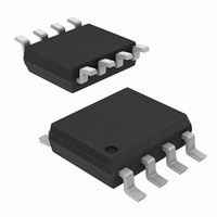
AD8314ARM-REEL Analog Devices Inc, AD8314ARM-REEL Datasheet - Page 12

AD8314ARM-REEL
Manufacturer Part Number
AD8314ARM-REEL
Description
IC RF DETECTOR\CTRLR 8-MSOP T/R
Manufacturer
Analog Devices Inc
Datasheet
1.AD8314ACPZ-RL7.pdf
(20 pages)
Specifications of AD8314ARM-REEL
Rohs Status
RoHS non-compliant
Frequency
100MHz ~ 2.7GHz
Rf Type
Cellular, GSM, TDMA, CDMA
Input Range
-45dBm ~ 0dBm
Voltage - Supply
2.7 V ~ 5.5 V
Current - Supply
5.7mA
Package / Case
8-TSSOP, 8-MSOP (0.118", 3.00mm Width)
Operating Temperature (min)
-40C
Operating Temperature (max)
85C
Operating Temperature Classification
Industrial
Mounting
Surface Mount
Pin Count
8
Package Type
MSOP
Accuracy
-
Lead Free Status / RoHS Status
Not Compliant
Available stocks
Company
Part Number
Manufacturer
Quantity
Price
Company:
Part Number:
AD8314ARM-REEL7
Manufacturer:
AD
Quantity:
5 379
Part Number:
AD8314ARM-REEL7
Manufacturer:
ADI/亚德诺
Quantity:
20 000
AD8314
APPLICATIONS
BASIC CONNECTIONS
Figure 31 shows connections for the basic measurement mode.
A supply voltage of 2.7 V to 5.5 V is required. The supply to the
VPOS pin should be decoupled with a low inductance 0.1 μF
surface-mount ceramic capacitor. A series resistor of about 10 Ω
can be added; this resistor slightly reduces the supply voltage to the
AD8314 (maximum current into the VPOS pin is approximately
9 mA when V_DN is delivering 5 mA). Its use should be
avoided in applications where the power supply voltage is very
low (that is, 2.7 V). A series inductor provides similar power
supply filtering with minimal drop in supply voltage.
The ENBL pin is here connected to VPOS. The AD8314 can be
disabled by pulling this pin to ground when the chip current is
reduced to about 20 μA from its normal value of 4.5 mA. The
logic threshold is around +V
in about 1.5 μs. Note, however, further settling time is generally
needed at low input levels.
The AD8314 has an internal input coupling capacitor. This
eliminates the need for external ac coupling. A broadband input
match is achieved in this example by connecting a 52.3 Ω resistor
between RFIN and ground. This resistance combines with the
internal input impedance of approximately 3 kΩ to give an
overall broadband input resistance of 50 Ω. Several other
coupling methods are possible, which are described in the
The measurement mode is selected by connecting VSET to
V_UP, which establishes a feedback path and sets the
logarithmic slope to its nominal value. The peak voltage range
of the measurement extends from −58 dBV to −13 dBV at
0.9 GHz, and only slightly less at higher frequencies up to
2.5 GHz. Therefore, using the 50 Ω termination, the equivalent
power range is −45 dBm to 0 dBm. At a slope of 21.5 mV/dB,
this would amount to an output span of 967 mV. Figure 32
shows the transfer function for V_UP at a supply voltage of 3 V
and input frequency of 0.9 GHz.
Input Coupling Options section.
INPUT
Figure 31. Basic Connections for Operation in Measurement Mode
(SEE TEXT)
OPTIONAL
52.3Ω
C
F
V
S
1
2
3
4
RFIN
ENBL
VSET
FLTR
AD8314
S
/2 and the enable function occurs
COMM
VPOS
V_DN
V_UP
8
7
6
5
0.1µF
OPTIONAL
(SEE TEXT)
V
V
V
UP
S
DN
Rev. B | Page 12 of 20
V_DN, which is generally not used when the AD8314 is used in
measurement mode, is essentially an inverted version of V_UP.
The voltage on V_UP and V_DN are related by
While V_DN can deliver up to 6 mA, the load resistance on
V_UP should not be lower than 10 kΩ in order that the full-
scale output of 1 V can be generated with the limited available
current of 200 μA maximum. Figure 32 shows the logarithmic
conformance under the same conditions.
TRANSFER FUNCTION IN TERMS OF SLOPE AND
INTERCEPT
The transfer function of the AD8314 is characterized in terms
of its slope and intercept. The logarithmic slope is defined as the
change in the RSSI output voltage for a 1 dB change at the input.
For the AD8314, slope is nominally 21.5 mV/dB. Therefore, a
10 dB change at the input results in a change at the output of
approximately 215 mV. Log conformance plot, Figure 32, shows
the range over which the device maintains its constant slope.
The dynamic range can be defined as the range over which the
error remains within a certain band, usually ±1 dB or ±3 dB. In
Figure 32 for example, the ±1 dB dynamic range is approximately
50 dB (from −13 dBV to −63 dBV).
V
1.2
1.0
0.8
0.6
0.4
0.2
DN
0
–70
= 2.25 V − 2 V
(–47dBm)
–60
Figure 32. V
V
R
S
T
= 3V
= 52.3Ω
Input Level vs. Input Level at 900 MHz
INTERCEPT
±1dB DYNAMIC RANGE
–50
INPUT AMPLITUDE (dBV)
UP
UP
±3dB DYNAMIC RANGE
and Log Conformance Error vs.
–40
–30
–20
(+3dBm)
–10
0
3
2
1
0
–1
–2
–3


