ATAVR128RFA1-EK1 Atmel, ATAVR128RFA1-EK1 Datasheet - Page 6
ATAVR128RFA1-EK1
Manufacturer Part Number
ATAVR128RFA1-EK1
Description
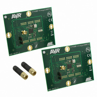
BOARD EVAL 802.15.4 ATMEGA128
Manufacturer
Atmel
Type
Microcontroller, Transceiverr
Datasheets
1.ATAVR128RFA1-EK1.pdf
(13 pages)
2.ATAVR128RFA1-EK1.pdf
(4 pages)
3.ATAVR128RFA1-EK1.pdf
(555 pages)
4.ATAVR128RFA1-EK1.pdf
(1 pages)
Specifications of ATAVR128RFA1-EK1
Frequency
2.4GHz
Silicon Manufacturer
Atmel
Silicon Family Name
ATmega
Kit Contents
Board
Svhc
No SVHC (15-Dec-2010)
Core Architecture
ATmega
Mcu Supported Families
ATMEGA128RFA1
Rohs Compliant
Yes
For Use With/related Products
ATMEGA128RF
Lead Free Status / RoHS Status
Lead free / RoHS Compliant
Other names
ATMEGA128RFA1-EK1
ATMEGA128RFA1-EK1
ATMEGA128RFA1-EK1


3.2.10 Port F (PF7...PF0)
3.2.11 Port G (PG5…PG0)
3.2.12 AVSS_RFP
3.2.13 AVSS_RFN
3.2.14 RFP
3.2.15 RFN
3.2.16 RSTN
3.2.17 RSTON
3.2.18 XTAL1
3.2.19 XTAL2
3.2.20 AREF
3.2.21 TST
3.2.22 CLKI
3.3 Unused Pins
6
ATmega128RFA1
Port F is an 8-bit bi-directional I/O port with internal pull-up resistors (selected for each
bit). The Port F output buffers have symmetrical drive characteristics with both high sink
and source capability. As inputs, Port F pins that are externally pulled low will source
current if the pull-up resistors are activated. The Port F pins are tri-stated when a reset
condition becomes active, even if the clock is not running.
Port F also provides functions of various special features of the ATmega128RFA1.
Port G is a 6-bit bi-directional I/O port with internal pull-up resistors (selected for each
bit). The Port G output buffers have symmetrical drive characteristics with both high
sink and source capability. However the driver strength of PG3 and PG4 is reduced
compared to the other port pins. The output voltage drop (V
leakage current is smaller. As inputs, Port G pins that are externally pulled low will
source current if the pull-up resistors are activated. The Port G pins are tri-stated when
a reset condition becomes active, even if the clock is not running.
Port G also provides functions of various special features of the ATmega128RFA1.
AVSS_RFP is a dedicated ground pin for the bi-directional, differential RF I/O port.
AVSS_RFN is a dedicated ground pin for the bi-directional, differential RF I/O port.
RFP is the positive terminal for the bi-directional, differential RF I/O port.
RFN is the negative terminal for the bi-directional, differential RF I/O port.
Reset input. A low level on this pin for longer than the minimum pulse length will
generate a reset, even if the clock is not running. Shorter pulses are not guaranteed to
generate a reset.
Reset output. A low level on this pin indicates a reset initiated by the internal reset
sources or the pin RSTN.
Input to the inverting 16MHz crystal oscillator amplifier. In general a crystal between
XTAL1 and XTAL2 provides the 16MHz reference clock of the radio transceiver.
Output of the inverting 16MHz crystal oscillator amplifier.
Reference voltage output of the A/D Converter. In general this pin is left open.
Programming and test mode enable pin. If pin TST is not used pull it to low.
Input to the clock system. If selected, it provides the operating clock of the
microcontroller.
Floating pins can cause power dissipation in the digital input stage. They should be
connected to an appropriate source. In normal operation modes the internal pull-up
OH
, V
OL
8266BS-MCU Wireless-03/11
) is higher while the
Related parts for ATAVR128RFA1-EK1
Image
Part Number
Description
Manufacturer
Datasheet
Request
R

Part Number:
Description:
DEV KIT FOR AVR/AVR32
Manufacturer:
Atmel
Datasheet:

Part Number:
Description:
INTERVAL AND WIPE/WASH WIPER CONTROL IC WITH DELAY
Manufacturer:
ATMEL Corporation
Datasheet:
Part Number:
Description:
Low-Voltage Voice-Switched IC for Hands-Free Operation
Manufacturer:
ATMEL Corporation
Datasheet:
Part Number:
Description:
MONOLITHIC INTEGRATED FEATUREPHONE CIRCUIT
Manufacturer:
ATMEL Corporation
Datasheet:
Part Number:
Description:
AM-FM Receiver IC U4255BM-M
Manufacturer:
ATMEL Corporation
Datasheet:
Part Number:
Description:
Monolithic Integrated Feature Phone Circuit
Manufacturer:
ATMEL Corporation
Datasheet:
Part Number:
Description:
Multistandard Video-IF and Quasi Parallel Sound Processing
Manufacturer:
ATMEL Corporation
Datasheet:
Part Number:
Description:
High-performance EE PLD
Manufacturer:
ATMEL Corporation
Datasheet:
Part Number:
Description:
8-bit Flash Microcontroller
Manufacturer:
ATMEL Corporation
Datasheet:
Part Number:
Description:
2-Wire Serial EEPROM
Manufacturer:
ATMEL Corporation
Datasheet: