RF3375PCK-410 RFMD, RF3375PCK-410 Datasheet - Page 3
RF3375PCK-410
Manufacturer Part Number
RF3375PCK-410
Description
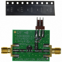
KIT EVAL FOR RF3375
Manufacturer
RFMD
Type
Amplifierr
Datasheet
1.RF3375TR7.pdf
(7 pages)
Specifications of RF3375PCK-410
Frequency
0Hz ~ 6GHz
For Use With/related Products
RF3375
Lead Free Status / RoHS Status
Lead free / RoHS Compliant
Other names
689-1045


DRAFT
DS101122
Pin
1
2
3
4
Function
RF OUT
RF IN
GND
GND
Description
RF input pin. This pin is NOT internally DC blocked. A DC blocking capacitor,
suitable for the frequency of operation, should be used in most applica-
tions. DC coupling of the input is not allowed, because this will override the
internal feedback loop and cause temperature instability.
Ground connection.
RF output and bias pin. Biasing is accomplished with an external series
resistor and choke inductor to V
current into this pin to a desired level. The resistor value is determined by
the following equation:
Care should also be taken in the resistor selection to ensure that the cur-
rent into the part never exceeds 80mA over the planned operating temper-
ature. This means that a resistor between the supply and this pin is always
required, even if a supply near 5.0V is available, to provide DC feedback to
prevent thermal runaway. Because DC is present on this pin, a DC blocking
capacitor, suitable for the frequency of operation, should be used in most
applications. The supply side of the bias network should also be well
bypassed.
Ground connection.
3.10
2.90
0.48
0.36
2 PL
Dimensions in mm.
Shaded lead is pin 1.
7628 Thorndike Road, Greensboro, NC 27409-9421 · For sales or technical
support, contact RFMD at (+1) 336-678-5570 or sales-support@rfmd.com.
1.04
0.80
R
2.60
2.40
=
Package Drawing
------------------------------------------------------ -
V
SUPPLY
CC
0.50
0.30
4.60
4.40
. The resistor is selected to set the DC
0.43
0.38
I
CC
–
V
1.75
1.40
DEVICE
1.60
1.40
1.80
1.45
DRAFT
0.53
0.41
Interface Schematic
RF IN
RF3375
RF OUT
3 of 7
Related parts for RF3375PCK-410
Image
Part Number
Description
Manufacturer
Datasheet
Request
R

Part Number:
Description:
IC AMP HBT GAAS CATV 8-SOIC
Manufacturer:
RFMD
Datasheet:

Part Number:
Description:
IC AMP MMIC GAAS 12GHZ 4-MICROX
Manufacturer:
RFMD
Datasheet:

Part Number:
Description:
IC AMP 3V LOW-NOISE SOT23-6
Manufacturer:
RFMD
Datasheet:

Part Number:
Description:
KIT EVAL FOR NBB-310
Manufacturer:
RFMD
Datasheet:
Part Number:
Description:
IC AMPLIFIER MMIC LNA 8-QFN
Manufacturer:
RFMD
Datasheet:
Part Number:
Description:
IC AMP MMIC GAAS 4GHZ 4-MICROX
Manufacturer:
RFMD
Datasheet:
Part Number:
Description:
IC SWITCH 10W PHEMT SPDT 12QFN
Manufacturer:
RFMD
Datasheet:
Part Number:
Description:
IC QUADRATURE MODULATOR 16-SOIC
Manufacturer:
RFMD
Datasheet:
Part Number:
Description:
100MHZ TO 4000MHZ, GAAS PHEMT MMIC LOW NOISE AMPLIFIERS
Manufacturer:
RFMD
Part Number:
Description:
KIT EVAL FOR RF2336
Manufacturer:
RFMD
Datasheet:


Part Number:
Description:
IC AMP WLAN/LNA DVR 3V SOT23-5
Manufacturer:
RFMD
Datasheet:

Part Number:
Description:
IC AMP HBT GAAS LNA BYPASS 8-QFN
Manufacturer:
RFMD
Datasheet:

Part Number:
Description:
IC AMP MMIC GAAS 10GHZ 4-MICROX
Manufacturer:
RFMD
Datasheet: