OM7614/BGM1011 NXP Semiconductors, OM7614/BGM1011 Datasheet - Page 4
OM7614/BGM1011
Manufacturer Part Number
OM7614/BGM1011
Description
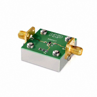
EVAL BOARD FOR BGM1011
Manufacturer
NXP Semiconductors
Type
Amplifierr
Datasheet
1.BGM1011115.pdf
(11 pages)
Specifications of OM7614/BGM1011
Frequency
0Hz ~ 4GHz
For Use With/related Products
BGM1011
Lead Free Status / RoHS Status
Not applicable / Not applicable
Other names
568-4096


Philips Semiconductors
APPLICATION INFORMATION
Figure 2 shows a typical application circuit for the BGM1011 MMIC. The device is internally matched to 50 Ω, and
therefore does not need any external matching. The value of the input and output DC blocking capacitors C1, C2 should
be not more than 100 pF for applications above 100 MHz. Their values can be used to fine tune the input and output
impedance. However, when the device is operated below 100 MHz, the capacitor value should be increased.
The nominal value of the RF choke, L1 is 100 nH. At frequencies below 100 MHz this value should be increased to
200 nH. At frequencies between 1 and 3 GHz a much lower value must be used (e.g. 18 nH) to improve return losses.
For optimal results, a good quality chip inductor such as the TDK MLG 1608 (0603), or a wire-wound SMD type should
be chosen.
Capacitor, C4 and resistor, R1 are added for optimal supply decoupling.
Both the RF choke, L1 and the 22 nF supply decoupling capacitor, C3 should be located as closely as possible to the
MMIC.
Separate paths must be used for the ground planes of the ground pins GND1, GND2, and these paths must be as short
as possible. When using vias, use multiple vias per pin in order to limit ground path inductance.
List of components used for the typical application; an amplifier for LNB IF output.
2002 Jan 14
C1, C2
C3
C4
R1
L1
COMPONENT
MMIC wideband amplifier
Fig.2 Typical application circuit
RF in
multilayer ceramic chip capacitor
multilayer ceramic chip capacitor
multilayer ceramic chip capacitor
SMD resistor
SMD inductor
C
1
6 [In]
DESCRIPTION
4 [GND1]
Fig.2 Typical application circuit
1 [Vs]
BGM1011
SOT363
2,5 [GND2]
4
100 pF
22 nF
5.6 pF
10 to 200 nH
10 Ω
3 [Out]
C
R
4
1
VALUE
C
3
L
1
Vs
C
2
RF out
Preliminary specification
0603
0603
0603
0603
0603
DIMENSIONS.
BGM1011
Related parts for OM7614/BGM1011
Image
Part Number
Description
Manufacturer
Datasheet
Request
R

Part Number:
Description:
Amplifier IC Development Tools GP MMIC demo board
Manufacturer:
NXP Semiconductors
Datasheet:
Part Number:
Description:
NXP Semiconductors designed the LPC2420/2460 microcontroller around a 16-bit/32-bitARM7TDMI-S CPU core with real-time debug interfaces that include both JTAG andembedded trace
Manufacturer:
NXP Semiconductors
Datasheet:

Part Number:
Description:
NXP Semiconductors designed the LPC2458 microcontroller around a 16-bit/32-bitARM7TDMI-S CPU core with real-time debug interfaces that include both JTAG andembedded trace
Manufacturer:
NXP Semiconductors
Datasheet:
Part Number:
Description:
NXP Semiconductors designed the LPC2468 microcontroller around a 16-bit/32-bitARM7TDMI-S CPU core with real-time debug interfaces that include both JTAG andembedded trace
Manufacturer:
NXP Semiconductors
Datasheet:
Part Number:
Description:
NXP Semiconductors designed the LPC2470 microcontroller, powered by theARM7TDMI-S core, to be a highly integrated microcontroller for a wide range ofapplications that require advanced communications and high quality graphic displays
Manufacturer:
NXP Semiconductors
Datasheet:
Part Number:
Description:
NXP Semiconductors designed the LPC2478 microcontroller, powered by theARM7TDMI-S core, to be a highly integrated microcontroller for a wide range ofapplications that require advanced communications and high quality graphic displays
Manufacturer:
NXP Semiconductors
Datasheet:
Part Number:
Description:
The Philips Semiconductors XA (eXtended Architecture) family of 16-bit single-chip microcontrollers is powerful enough to easily handle the requirements of high performance embedded applications, yet inexpensive enough to compete in the market for hi
Manufacturer:
NXP Semiconductors
Datasheet:
Part Number:
Description:
The XA-S3 device is a member of Philips Semiconductors? XA(eXtended Architecture) family of high performance 16-bitsingle-chip microcontrollers
Manufacturer:
NXP Semiconductors
Datasheet:

Part Number:
Description:
The NXP BlueStreak LH75401/LH75411 family consists of two low-cost 16/32-bit System-on-Chip (SoC) devices
Manufacturer:
NXP Semiconductors
Datasheet:
Part Number:
Description:
The NXP LPC3130/3131 combine an 180 MHz ARM926EJ-S CPU core, high-speed USB2
Manufacturer:
NXP Semiconductors
Datasheet:
Part Number:
Description:
The NXP LPC3141 combine a 270 MHz ARM926EJ-S CPU core, High-speed USB 2
Manufacturer:
NXP Semiconductors
Part Number:
Description:
The NXP LPC3143 combine a 270 MHz ARM926EJ-S CPU core, High-speed USB 2
Manufacturer:
NXP Semiconductors

Part Number:
Description:
The NXP LPC3152 combines an 180 MHz ARM926EJ-S CPU core, High-speed USB 2
Manufacturer:
NXP Semiconductors
Part Number:
Description:
The NXP LPC3154 combines an 180 MHz ARM926EJ-S CPU core, High-speed USB 2
Manufacturer:
NXP Semiconductors