NLB-310-PCK RFMD, NLB-310-PCK Datasheet
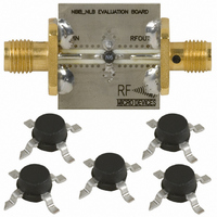
KIT EVAL FOR NLB-310

NLB-310-PCK

Manufacturer Part Number
NLB-310-PCK
Description
KIT EVAL FOR NLB-310
Manufacturer
RFMD
Type
Amplifierr
Datasheet

Specifications of NLB-310-PCK

Frequency
0Hz ~ 10GHz
For Use With/related Products
NLB-310
Lead Free Status / RoHS Status
Lead free / RoHS Compliant
Other names
689-1060

Available stocks

Company
Part Number
Manufacturer
Quantity
Price
Part Number:
NLB-310-PCK
Manufacturer:
RFMD
Quantity:
5 000
Product Description
The NLB-310 cascadable broadband InGaP/GaAs MMIC
amplifier is a low-cost, high-performance solution for gen-
eral purpose RF and microwave amplification needs. This
50Ω gain block is based on a reliable HBT proprietary
MMIC design, providing unsurpassed performance for
small-signal applications. Designed with an external bias
resistor, the NLB-310 provides flexibility and stability. The
NLB-310 is packaged in a low-cost, surface-mount plastic
package, providing ease of assembly for high-volume
tape-and-reel requirements.
Optimum Technology Matching® Applied
Rev A8 060412
Typical Applications
• Narrow and Broadband Commercial and
• Linear and Saturated Amplifiers
Si BJT
Si Bi-CMOS
InGaP/HBT
Military Radio Designs
RF IN
Functional Block Diagram
1
RoHS Compliant & Pb-Free Product
GaAs HBT
SiGe HBT
GaN HEMT
GND
GND
4
2
MARKING - N6
0
3
GaAs MESFET
Si CMOS
SiGe Bi-CMOS
RF OUT
RF OUT
• Gain Stage or Driver Amplifiers for
Seating Plane
MWRadio/Optical Designs (PTP/PMP/
LMDS/UNII/VSAT/WLAN/Cellular/DWDM)
Features
Ordering Information
RF Micro Devices, Inc.
7628 Thorndike Road
Greensboro, NC 27409, USA
• Reliable, Low-Cost HBT Design
• 12.7dB Gain, +12.6dBm P1dB@2GHz
• High P1dB of +14.9dBm@6.0GHz and
• Single Power Supply Operation
• 50Ω I/O Matched for High Freq. Use
NLB-310
NLB-310-T1
NLB-310-E
NBB-X-K1
+13.1dBm@10.0GHz
0.08 S
6
Package Style: Micro-X, 4-Pin, Plastic
GaAs MMIC AMPLIFIER DC TO 10GHz
S
D
A
1 J
L 3
B
C
N 5
E
Cascadable Broadband GaAs MMIC Amplifier DC to
10GHz
Tape & Reel, 1000 Pieces
Fully Assembled Evaluation Board
Extended Frequency InGaP Amp Designer’s Tool Kit
F
CASCADABLE BROADBAND
2
K x 3
G
4 M
H
0.1
Gauge Plane
NLB-310
1
2
3
4
5
NOTE: All dimensions are in millimeters, and
the dimensions in inches are for reference only.
G
M
A
B
C
D
E
F
H
J
K
L
N
0.436 0.510 0.586 0.017 0.020 0.023
0.535 0.660 0.785 0.021 0.026 0.031
Min.
2.39
2.19
1.91
1.32
0.10
0.05
0.65
0.85
4.53
4.73
MILLIMETERS
0.535 REF.
Nom. Max.
2.54
2.34
2.16
1.52
0.15
0.10
0.75
0.95
4.68
4.88
http://www.rfmd.com
Fax (336) 664 0454
Tel (336) 664 1233
2.69
2.49
2.41
1.72
0.20
0.15
0.85
1.05
4.83
5.03
0.094 0.100 0.106
0.086 0.092 0.098
0.075 0.085 0.095
0.052 0.060 0.068
0.004 0.006 0.008
0.002 0.004 0.006
0.025 0.029 0.033
0.033 0.037 0.041
0.178 0.184 0.190
0.186 0.192 0.198
Min.
0.021 REF.
INCHES
Nom. Max.
4-139

Related parts for NLB-310-PCK

NLB-310-PCK Summary of contents

Page 1

... HBT proprietary MMIC design, providing unsurpassed performance for small-signal applications. Designed with an external bias resistor, the NLB-310 provides flexibility and stability. The NLB-310 is packaged in a low-cost, surface-mount plastic package, providing ease of assembly for high-volume tape-and-reel requirements. ...

Page 2

... NLB-310 Absolute Maximum Ratings Parameter RF Input Power Power Dissipation Device Current Channel Temperature Operating Temperature Storage Temperature Exceeding any one or a combination of these limits may cause permanent damage. Parameter Min. Overall Small Signal Power Gain, S21 12.0 Gain Flatness, GF Input VSWR ...

Page 3

... Because DC is present on this pin blocking capacitor, suit- able for the frequency of operation, should be used in most applications. The supply side of the bias network should also be well bypassed. 4 GND Same as pin 2. Rev A8 060412 . The resistor is selected to set the – DEVICE ------------------------------------------ - NLB-310 Interface Schematic RF OUT RF IN 4-141 ...

Page 4

... NLB-310 Application notes related to biasing circuit, device footprint, and thermal considerations are available on request. In Recommended Bias Resistor Values Supply Voltage Bias Resistor, R (Ω 4-142 Typical Bias Configuration block 100 140 200 choke (optional) Out C block DEVICE 20 300 Rev A8 060412 ...

Page 5

... Extended Frequency InGaP Amplifier Designer’s Tool Kit This tool kit was created to assist in the design-in of the RFMD NBB- and NLB-series InGap HBT gain block amplifiers. Each tool kit contains the following. • 5 each NBB-300, NBB-310 and NBB-400 Ceramic Micro-X Amplifiers • ...

Page 6

... NLB-310 FLANGE HUB All dimensions in mm 0.30 ± 0.05 R0.3 MAX. SECTION A-A NOTES sprocket hole pitch cumulative tolerance ±0.2. 2. Camber not to exceed 100 mm. 3. Material: PS+ and Bo measured on a plane 0.3 mm above the bottom of the pocket measured from a plane on the inside bottom of the pocket to the surface of the carrier. ...

Page 7

... NLB-310 S21 versus Frequency, Over Temperature 1.0 2.0 3.0 4.0 5.0 6.0 7.0 8.0 9.0 10.0 11.0 12.0 Frequency (GHz) S22 versus Frequency, Over Temperature 1.0 2 ...

Page 8

... NLB-310 Note: The s-parameter gain results shown include device performance as well as evaluation board and connector loss variations. The insertion losses of the evaluation board and connectors are as follows: 1GHz to 4GHz=-0.06dB 5GHz to 9GHz=-0.22dB 10GHz to 14GHz=-0.50dB 15GHz to 20GHz=-1.08dB 4-146 Rev A8 060412 ...

Related keywords