CYRF6936-40LFXC Cypress Semiconductor Corp, CYRF6936-40LFXC Datasheet - Page 2
CYRF6936-40LFXC
Manufacturer Part Number
CYRF6936-40LFXC
Description
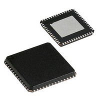
IC WIRELESS USB LP 40VQFN
Manufacturer
Cypress Semiconductor Corp
Datasheet
1.CYRF6936-40LFXC.pdf
(23 pages)
Specifications of CYRF6936-40LFXC
Frequency
2.4GHz
Data Rate - Maximum
1Mbps
Modulation Or Protocol
DSSS, GFSK
Applications
Remote Control
Power - Output
4dBm
Sensitivity
-97dBm
Voltage - Supply
1.8 V ~ 3.6 V
Current - Receiving
21.2mA
Current - Transmitting
34mA
Data Interface
PCB, Surface Mount
Antenna Connector
PCB, Surface Mount
Operating Temperature
0°C ~ 70°C
Package / Case
40-VQFN Exposed Pad, 40-HVQFN, 40-SQFN, 40-DHVQFN
Interface
SPI
Termination Type
SMD
Bandwidth
876kHz
Supply Voltage Max
3.6V
Data Rate Max
1000Kbps
Frequency Band Type
ISM
Features
10
Frequency Band Range
2.400 - 2.483 GHz
Supply Voltage Min
2.4V
Lead Free Status / RoHS Status
Lead free / RoHS Compliant
Memory Size
-
Lead Free Status / Rohs Status
Lead free / RoHS Compliant
Other names
428-2024
CYRF6936-40LFXC
CYRF6936-40LFXC
Available stocks
Company
Part Number
Manufacturer
Quantity
Price
Company:

Part Number:
CYRF6936-40LFXC
Manufacturer:
CYPRESS
Quantity:
210
Part Number:
CYRF6936-40LFXC
Manufacturer:
CRIIUS
Quantity:
20 000


Document #: 38-16015 Rev. *H
Functional Description
The CYRF6936 WirelessUSB™ LP radio is a second generation member of the Cypress WirelessUSB Radio System-On-Chip
(SoC) family. The CYRF6936 is interoperable with the first generation CYWUSB69xx devices. The CYRF6936 IC adds a range
of enhanced features, including increased operating voltage range, reduced supply current in all operating modes, higher data
rate options, reduced crystal start up, synthesizer settling, and link turnaround times.
Table 1. Pin Description
1
2, 4, 5, 9, 14, 15, 17, 18,
20, 21, 22, 23, 31, 32,
36, 39
3, 7, 16
6, 8, 38
10
11
12
13
19
24
25
26
27
28
29
30
33
Pin Number
XTAL
NC
V
V
RF
RF
GND
RF
RESV
SS
SCK
IRQ
MOSI
MISO
XOUT
PACTL
V
CC
BAT(0-2)
IO
Name
BIAS
P
N
RF
XTAL
Type
V
V
GND
Pwr
Pwr
Pwr
Figure 1. Pin Diagram - CYRF6936 40 QFN
NC
V
BAT1
V
BAT2
Corner
NC
NC
NC
NC
BIAS
IO
IO
IO
IO
IO
IO
IO
O
tabs
CC
CC
I
I
I
I
10
1
2
3
4
5
6
7
8
9
Default
O
O
O
O
Z
I
I
I
I
I
I
WirelessUSB LP
12 MHz crystal.
Connect to GND.
V
V
RF IO 1.8V reference voltage.
Differential RF signal to and from antenna.
Ground.
Differential RF signal to and from antenna.
Must be connected to GND.
SPI enable, active LOW assertion. Enables and frames transfers.
SPI clock.
Interrupt output (configurable active HIGH or LOW), or GPIO.
SPI data input pin (Master Out Slave In), or SDAT.
SPI data output pin (Master In Slave Out), or GPIO (in SPI 3-pin mode).
Tri-states when SPI 3PIN = 0 and SS is deasserted.
Buffered 0.75, 1.5, 3, 6, or 12 MHz clock, PACTL, or GPIO.
Tri-states in sleep mode (configure as GPIO drive LOW).
Control signal for external PA, T/R switch, or GPIO.
IO interface voltage, 1.8–3.6V.
40-Pin QFN
CYRF6936
* E-PAD Bottom Side
CC
BAT
= 2.4V to 3.6V. Typically connected to V
= 1.8V to 3.6V. Main supply.
30
29
28
27
26
25
24
23
22
21
PACTL / GPIO
XOUT / GPIO
MISO / GPIO
MOSI / SDAT
IRQ / GPIO
SCK
SS
NC
NC
NC
Description
REG.
CYRF6936
Page 2 of 23
[+] Feedback
Related parts for CYRF6936-40LFXC
Image
Part Number
Description
Manufacturer
Datasheet
Request
R

Part Number:
Description:
IC WIRELESS USB LP 2.4GHZ 40VQFN
Manufacturer:
Cypress Semiconductor Corp
Datasheet:

Part Number:
Description:
Manufacturer:
Cypress Semiconductor Corp
Datasheet:
Part Number:
Description:
Manufacturer:
Cypress Semiconductor Corp
Datasheet:
Part Number:
Description:
Manufacturer:
Cypress Semiconductor Corp
Datasheet:
Part Number:
Description:
Manufacturer:
Cypress Semiconductor Corp
Datasheet:
Part Number:
Description:
Manufacturer:
Cypress Semiconductor Corp
Datasheet: