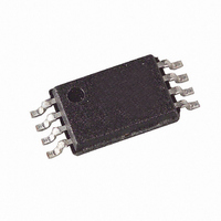
T48C862M-R3-TNQ Atmel, T48C862M-R3-TNQ Datasheet - Page 33

T48C862M-R3-TNQ
Manufacturer Part Number
T48C862M-R3-TNQ
Description
IC MON TIRE PRESS 315MHZ 24SOIC
Manufacturer
Atmel
Datasheet
1.T48C862M-R3-TNS.pdf
(107 pages)
Specifications of T48C862M-R3-TNQ
Frequency
315MHz
Modulation Or Protocol
FM, FSK
Data Rate - Maximum
32 kBaud
Power - Output
10dBm
Current - Transmitting
9.5mA
Data Interface
PCB, Surface Mount
Antenna Connector
PCB, Surface Mount
Memory Size
1KB EEPROM, 1KB RAM
Voltage - Supply
2 V ~ 4 V
Operating Temperature
-40°C ~ 125°C
Package / Case
24-SOIC (0.200", 5.30mm Width)
Lead Free Status / RoHS Status
Contains lead / RoHS non-compliant
Features
-
Applications
-
Bi-directional Ports
Bi-directional Port 1
4554A–4BMCU–02/03
With the exception of Port 1 and Port 6, all other ports (2, 4 and 5) are 4 bits wide. Port 1
and Port 6 have a data width of 2 bits (bit 0 and bit 3). All ports may be used for data
input or output. All ports are equipped with Schmitt trigger inputs and a variety of mask
options for open-drain, open-source, full-complementary outputs, pull-up and pull-down
transistors. All Port Data Registers (PxDAT) are I/O mapped to the primary address reg-
ister of the respective port address and the Port Control Register (PxCR), to the
corresponding auxiliary register.
There are five different directional ports available:
Port 1
Port 2
Port 5
Port 4
Port 6
In Port 1 the data direction register is not independently software programmable, the
direction of the complete port being switched automatically when an I/O instruction
occurs (see Figure 28). The port is switched to output mode via an OUT instruction and
to input via an IN instruction. The data written to a port will be stored into the output data
latches and appears immediately at the port pin following the OUT instruction. After
RESET all output latches are set to "1" and the port is switched to input mode. An IN
instruction reads the condition of the associated pins.
Note:
Care must be taken when switching the bi-directional port from output to input. The
capacitive pin loading at this port in conjunction with the high resistance pull-ups may
cause the CPU to read the contents of the output data register rather than the external
input state. To avoid this, one of the following programming techniques should be used:
Use two IN-instructions and DROP the first data nibble. The first IN switches the port
from output to input and the DROP removes the first invalid nibble. The second IN reads
the valid pin state.
Use an OUT-instruction followed by an IN-instruction. Via the OUT-instruction, the capac-
itive load is charged or discharged depending on the optional pull-up/pull-down
configuration. Write a "1" for pins with pull-up resistors and a "0" for pins with pull-down
resistors.
pull-ups and programmable interrupt logic.
interface to Timer 2, SSI, voltage monitor input and external interrupt input.
interface to Timer 3 and external interrupt input.
2-bit wide bi-directional port with automatic full bus width direction switching.
4-bit wide bitwise-programmable I/O port.
4-bit wide bitwise-programmable bi-directional port with optional strong
4-bit wide bitwise-programmable bi-directional port also provides the I/O
2-bit wide bitwise-programmable bi-directional port also provides the I/O
T48C862-R3
33


