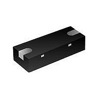
CDDFN2-T3.3LC Bourns Inc., CDDFN2-T3.3LC Datasheet - Page 3

CDDFN2-T3.3LC
Manufacturer Part Number
CDDFN2-T3.3LC
Description
TVS DIODE 3.3V BI SMD
Manufacturer
Bourns Inc.
Series
CDr
Datasheet
1.CDDFN2-T3.3LC.pdf
(4 pages)
Specifications of CDDFN2-T3.3LC
Package / Case
2-UFDFN
Voltage - Reverse Standoff (typ)
3V
Voltage - Breakdown
4V
Polarization
Bidirectional
Mounting Type
Surface Mount
Polarity
Bidirectional
Channels
1 Channel
Clamping Voltage
5 V
Operating Voltage
+/- 3.8 V
Breakdown Voltage
4 V to 6.5 V
Termination Style
SMD/SMT
Peak Surge Current
5 A
Capacitance
13 pF
Maximum Operating Temperature
+ 125 C
Minimum Operating Temperature
- 55 C
Dimensions
0.55 mm W x 0.95 mm L x 0.45 mm H
Mounting Style
SMD/SMT
Reverse Stand-off Voltage Vrwm
3.3V
Clamping Voltage Vc Max
8V
Diode Configuration
Bidirectional
Peak Pulse Current Ippm
5A
Diode Case Style
DFN
No. Of Pins
2
Breakdown Voltage Vbr
6.5V
Breakdown Voltage Min
4V
Lead Free Status / RoHS Status
Lead free / RoHS Compliant
Power (watts)
-
Lead Free Status / Rohs Status
Lead free / RoHS Compliant
Other names
CDDFN2-T3.3LCTR
Available stocks
Company
Part Number
Manufacturer
Quantity
Price
Part Number:
CDDFN2-T3.3LC
Manufacturer:
BOURNS/伯恩斯
Quantity:
20 000
Specifi cations are subject to change without notice.
Customers should verify actual device performance in their specifi c applications.
Performance Graphs
Pulse Waveform
Typical Capacitance Variation of C
16
14
12
10
CDDFN2-T3.3LC - Surface Mount TVS Diode
8
6
4
2
0
-4
120
100
80
60
40
20
0
-3
0
-2
5
t
t
-1
Input Voltage (V)
10
t
d
= t
e
t
|
0
Test Waveform Parameters
t
t
t – Time (µs)
I
15
t
d
PP
= 8 µs
= 20 µs
/2
IN
1
20
vs V
Pin 1 to Pin 2
f = 1 MHz,
T = 25 °C
IN
2
25
3
30
4
Overshoot & Clamping Voltage
Power Derating Curve
30
25
15
-5
5
-490.00 ns
100
2
80
60
40
20
0
0
ESD Test Pulse: 25 kilovolt, 1/30 ns (waveshape)
25
Ambient Temperature (°C)
50
Mounting on Glass Epoxy PCBs
10.00 ns
75
100
125
510.00 ns
150
0.2


