FDMC7692 Fairchild Semiconductor, FDMC7692 Datasheet

MOSFET N-CH 30V 8-MLP

FDMC7692

Manufacturer Part Number
FDMC7692
Description
MOSFET N-CH 30V 8-MLP
Manufacturer
Fairchild Semiconductor
Series
PowerTrench®r
Datasheet

Specifications of FDMC7692

Fet Type
MOSFET N-Channel, Metal Oxide
Fet Feature
Logic Level Gate
Rds On (max) @ Id, Vgs
8.5 mOhm @ 13.3A, 10V
Drain To Source Voltage (vdss)
30V
Current - Continuous Drain (id) @ 25° C
13.3A
Vgs(th) (max) @ Id
3V @ 250µA
Gate Charge (qg) @ Vgs
29nC @ 10V
Input Capacitance (ciss) @ Vds
1680pF @ 15V
Power - Max
2.3W
Mounting Type
Surface Mount
Package / Case
8-MLP, Power33
Configuration
Single
Transistor Polarity
N-Channel
Resistance Drain-source Rds (on)
9.5 mOhms
Forward Transconductance Gfs (max / Min)
60 S
Drain-source Breakdown Voltage
30 V
Continuous Drain Current
16 A
Power Dissipation
2.3 W
Maximum Operating Temperature
+ 150 C
Mounting Style
SMD/SMT
Minimum Operating Temperature
- 55 C
Lead Free Status / RoHS Status
Lead free / RoHS Compliant

Available stocks

Company
Part Number
Manufacturer
Quantity
Price
Part Number:
FDMC7692
Manufacturer:
FAIRCHILD/仙童
Quantity:
20 000
Company:
Part Number:
FDMC7692
Quantity:
200
Part Number:
FDMC7692S
Manufacturer:
FAIRCHILD
Quantity:
2 766
Part Number:
FDMC7692S
Manufacturer:
FAIRCHILD
Quantity:
8 000
Part Number:
FDMC7692S
Manufacturer:
FAIRCHILD/ON
Quantity:
20 000
©2010 Fairchild Semiconductor Corporation
FDMC7692 Rev.C
FDMC7692
N-Channel Power Trench
30 V, 13.3 A, 8.5 m:
Features
„ Max r
„ Max r
„ High performance technology for extremely low r
„ Termination is Lead-free and RoHS Compliant
MOSFET Maximum Ratings
Thermal Characteristics
Package Marking and Ordering Information
V
V
I
E
P
T
R
R
D
DS
GS
AS
D
J
TJC
TJA
, T
Symbol
Device Marking
STG
FDMC7692
DS(on)
DS(on)
= 8.5 m: at V
= 11.5 m: at V
Drain to Source Voltage
Gate to Source Voltage
Drain Current -Continuous (Package limited)
Single Pulse Avalanche Energy
Power Dissipation
Power Dissipation
Operating and Storage Junction Temperature Range
Thermal Resistance, Junction to Case
Thermal Resistance, Junction to Ambient
Top
GS
GS
MLP 3.3x3.3
= 10 V, I
FDMC7692
= 4.5 V, I
-Continuous
-Pulsed
Device
D
D
= 13.3 A
= 10.6 A
Pin 1
T
A
®
= 25 °C unless otherwise noted
DS(on)
S
Parameter
MOSFET
S
S
MLP 3.3x3.3
G
Package
Bottom
1
T
T
T
T
General Description
This
Semiconductor’s advanced Power Trench
been especially tailored to minimize the on-state resistance. This
device is well suited for Power Management and load switching
applications common in Notebook Computers and Portable
Battery Packs.
Application
„ DC - DC Buck Converters
„ Notebook battery power management
„ Load switch in Notebook
D
A
C
A
C
= 25 °C
= 25 °C
= 25 °C
D
= 25 °C
D
N-Channel
D
Reel Size
13 ’’
(Note 1a)
(Note 1a)
(Note 1a)
(Note 3)
D
D
D
D
MOSFET
8
5
6
7
Tape Width
12 mm
is produced using Fairchild
-55 to +150
Ratings
13.3
±20
2.3
4.3
53
30
16
40
58
29
®
September 2010
process that has
www.fairchildsemi.com
3000 units
Quantity
1
4
3
2
G
S
S
Units
S
°C/W
mJ
°C
W
V
V
A

Related parts for FDMC7692

FDMC7692 Summary of contents

Page 1

... Thermal Resistance, Junction to Case TJC R Thermal Resistance, Junction to Ambient TJA Package Marking and Ordering Information Device Marking Device FDMC7692 FDMC7692 ©2010 Fairchild Semiconductor Corporation FDMC7692 Rev.C ® MOSFET General Description = 13.3 A This N-Channel D Semiconductor’s advanced Power Trench = 10 been especially tailored to minimize the on-state resistance. This ...

Page 2

... Reverse Recovery Charge rr NOTES determined with the device mounted TJA the user's board design. 2. Pulse Test: Pulse Width < 300 Ps, Duty cycle < 2 based on starting mH ©2010 Fairchild Semiconductor Corporation FDMC7692 Rev °C unless otherwise noted J Test Conditions = 250 PA 250 PA, referenced to 25 ° ...

Page 3

... T J Figure 3. Normalized On- Resistance vs Junction Temperature 40 P PULSE DURATION = 80 s DUTY CYCLE = 0.5% MAX 150 GATE TO SOURCE VOLTAGE (V) GS Figure 5. Transfer Characteristics ©2010 Fairchild Semiconductor Corporation FDMC7692 Rev °C unless otherwise noted J 4 3.5 3 3.5 V 2.5 GS 2.0 1 1.0 0 100 125 150 ...

Page 4

... Unclamped Inductive Switching Capability THIS AREA IS LIMITED BY r DS(on) SINGLE PULSE 0 MAX RATED 125 C 0.01 0.01 0 DRAIN to SOURCE VOLTAGE (V) DS Figure 11. Forward Bias Safe Operating Area ©2010 Fairchild Semiconductor Corporation FDMC7692 Rev °C unless otherwise noted J 3000 1000 100 100 Figure 10. ...

Page 5

... Typical Characteristics 2 DUTY CYCLE-DESCENDING ORDER 0.5 0.2 0.1 0.05 0.1 0.02 0.01 0.01 SINGLE PULSE 0.001 - ©2010 Fairchild Semiconductor Corporation FDMC7692 Rev °C unless otherwise noted 125 C RECTANGULAR PULSE DURATION (sec) Figure 13. Transient Thermal Response Curve NOTES: DUTY FACTOR PEAK TJA ...

Page 6

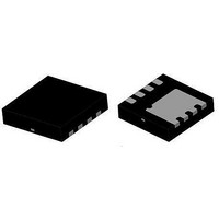
... Dimensional Outline and Pad Layout ©2010 Fairchild Semiconductor Corporation FDMC7692 Rev.C 6 www.fairchildsemi.com ...

Page 7

... Datasheet Identification Product Status Advance Information Formative / In Design Preliminary First Production No Identification Needed Full Production Obsolete Not In Production ©2010 Fairchild Semiconductor Corporation FDMC7692 Rev.C Power-SPM™ ® ® PowerTrench SM PowerXS™ Programmable Active Droop™ ® QFET QS™ Quiet Series™ ...

Related keywords