FCA16N60N Fairchild Semiconductor, FCA16N60N Datasheet

MOSFET N-CH 600V TO-3PN

FCA16N60N

Manufacturer Part Number
FCA16N60N
Description
MOSFET N-CH 600V TO-3PN
Manufacturer
Fairchild Semiconductor
Series
SupreMOS™r
Datasheet

Specifications of FCA16N60N

Fet Type
MOSFET N-Channel, Metal Oxide
Fet Feature
Standard
Rds On (max) @ Id, Vgs
199 mOhm @ 8A, 10V
Drain To Source Voltage (vdss)
600V
Current - Continuous Drain (id) @ 25° C
16A
Vgs(th) (max) @ Id
4V @ 250µA
Gate Charge (qg) @ Vgs
52.3nC @ 10V
Input Capacitance (ciss) @ Vds
2170pF @ 100V
Power - Max
134.4W
Mounting Type
Through Hole
Package / Case
TO-3PN
Configuration
Single
Transistor Polarity
N-Channel
Resistance Drain-source Rds (on)
0.17 Ohms
Forward Transconductance Gfs (max / Min)
20 S
Drain-source Breakdown Voltage
600 V
Continuous Drain Current
16 A
Power Dissipation
134.4 W
Maximum Operating Temperature
+ 150 C
Mounting Style
Through Hole
Minimum Operating Temperature
- 55 C
Lead Free Status / RoHS Status
Lead free / RoHS Compliant
©2009 Fairchild Semiconductor Corporation
FCA16N60N Rev. A1
MOSFET Maximum Ratings
Thermal Characteristics
V
V
I
I
E
I
E
dv/dt
P
T
T
*Drain current limited by maximum junction temperature
R
R
R
D
DM
AR
FCA16N60N
N-Channel MOSFET
600V, 16A, 0.170
Features
• R
• Ultra low gate charge ( Typ. Qg = 40.2nC)
• Low effective output capacitance
• 100% avalanche tested
• RoHS compliant
J
L
DSS
GSS
AS
AR
D
, T
JC
CS
JA
Symbol
Symbol
STG
DS(on)
= 0.17
Drain to Source Voltage
Gate to Source Voltage
Drain Current
Drain Current
Single Pulsed Avalanche Energy
Avalanche Current
Repetitive Avalanche Energy
MOSFET dv/dt Ruggedness
Peak Diode Recovery dv/dt
Power Dissipation
Operating and Storage Temperature Range
Maximum Lead Temperature for Soldering Purpose,
1/8” from Case for 5 Seconds
Thermal Resistance, Junction to Case
Thermal Resistance, Case to Heat Sink (Typical)
Thermal Resistance, Junction to Ambient
( Typ.)@ V
GS
= 10V, I
G
D
S
D
= 8A
T
C
= 25
Parameter
Parameter
-Continuous (T
-Continuous (T
- Pulsed
(T
- Derate above 25
C
o
C unless otherwise noted*
= 25
TO-3PN
FCA Series
o
C)
C
C
= 25
= 100
1
o
C
o
Description
The SupreMOS MOSFET, Fairchild’s next generation of high
voltage super-junction MOSFETs, employs a deep trench filling
process that differentiates it from preceding multi-epi based
technologies. By utilizing this advanced technology and precise
process control, SupreMOS provides world class Rsp, superior
switching performance and ruggedness.
This SupreMOS MOSFET fits the industry’s AC-DC SMPS
requirements for PFC, server/telecom power, FPD TV power,
ATX power, and industrial power applications.
C)
o
C)
(Note 1)
(Note 2)
(Note 3)
G
FCA16N60N
FCA16N60N
-55 to +150
134.4
16.0
10.1
48.0
1.34
1.08
0.93
0.24
600
±30
355
100
300
5.3
20
40
SupreMOS
S
D
www.fairchildsemi.com
August 2009
Units
W/
Units
o
V/ns
V/ns
C/W
mJ
mJ
o
o
W
V
V
A
A
A
C
C
o
C
TM

Related parts for FCA16N60N

FCA16N60N Summary of contents

Page 1

... R Thermal Resistance, Case to Heat Sink (Typical Thermal Resistance, Junction to Ambient JA ©2009 Fairchild Semiconductor Corporation FCA16N60N Rev. A1 Description = 8A The SupreMOS MOSFET, Fairchild’s next generation of high D voltage super-junction MOSFETs, employs a deep trench filling process that differentiates it from preceding multi-epi based technologies. By utilizing this advanced technology and precise process control, SupreMOS provides world class Rsp, superior switching performance and ruggedness ...

Page 2

... Q Reverse Recovery Charge rr Notes: 1. Repetitive Rating: Pulse width limited by maximum junction temperature 5.3A Starting 16A, di/dt 200A 380V, Starting Essentially Independent of Operating Temperature Typical Characteristics FCA16N60N Rev. A1 Package Reel Size TO-3PN - unless otherwise noted C Test Conditions I = 1mA 0V 1mA, Referenced 480V, V ...

Page 3

... Drain Current [A] D Figure 5. Capacitance Characteristics 10000 C iss = oss = rss = C gd 7500 C oss 5000 C 2500 iss C rss 0 0 Drain-Source Voltage [V] DS FCA16N60N Rev. A1 Figure 2. Transfer Characteristics 100 *Notes: 1. 250 s Pulse Test 0 Figure 4. Body Diode Forward Voltage 100 V = 10V 20V GS o *Notes: T ...

Page 4

... Single Pulse 0. Drain-Source Voltage [V] DS Figure 11. Transient Thermal Response Curve 2 1 0.5 0.2 0.1 0.1 0.05 0.02 0.01 Single pulse 0.01 0.005 -5 10 FCA16N60N Rev. A1 (Continued) Figure 8. On-Resistance Variation *Notes 1mA D 100 150 200 100 s 1ms 10ms 150 C 100 1000 ...

Page 5

... FCA16N60N Rev. A1 Gate Charge Test Circuit & Waveform Resistive Switching Test Circuit & Waveforms Unclamped Inductive Switching Test Circuit & Waveforms 5 www.fairchildsemi.com ...

Page 6

... FCA16N60N Rev. A1 Peak Diode Recovery dv/dt Test Circuit & Waveforms + + • • • I • www.fairchildsemi.com ...

Page 7

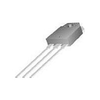
... Mechanical Dimensions FCA16N60N Rev. A1 TO-3PN 7 Dimensions in Millimeters www.fairchildsemi.com ...

Page 8

... TRADEMARKS The following includes registered and unregistered trademarks and service marks, owned by Fairchild Semiconductor and/or its global subsidiaries, and is not intended exhaustive list of all such trademarks. AccuPower™ FPS™ Auto-SPM™ F-PFS™ FRFET Build it Now™ CorePLUS™ Global Power Resource CorePOWER™ ...

Related keywords