FCH47N60F_F133 Fairchild Semiconductor, FCH47N60F_F133 Datasheet

MOSFET N-CH 600V 47A TO-247

FCH47N60F_F133

Manufacturer Part Number
FCH47N60F_F133
Description
MOSFET N-CH 600V 47A TO-247
Manufacturer
Fairchild Semiconductor
Series
SupreMOS™r
Datasheet

Specifications of FCH47N60F_F133

Fet Type
MOSFET N-Channel, Metal Oxide
Fet Feature
Standard
Rds On (max) @ Id, Vgs
73 mOhm @ 23.5A, 10V
Drain To Source Voltage (vdss)
600V
Current - Continuous Drain (id) @ 25° C
47A
Vgs(th) (max) @ Id
5V @ 250µA
Gate Charge (qg) @ Vgs
270nC @ 10V
Input Capacitance (ciss) @ Vds
8000pF @ 25V
Power - Max
417W
Mounting Type
Through Hole
Package / Case
TO-247-3
Lead Free Status / RoHS Status
Lead free / RoHS Compliant

Available stocks

Company
Part Number
Manufacturer
Quantity
Price
Company:
Part Number:
FCH47N60F_F133FCH47N60F-F133
Quantity:
2 500
Part Number:
FCH47N60F_F133
Manufacturer:
FSC可看货
Quantity:
20 000
©2009 Fairchild Semiconductor Corporation
FCH47N60F _F133 Rev. A.
FCH47N60F
600V N-Channel MOSFET
Features
• 650V @T
• Typ. R
• Fast Recovery Type ( t
• Ultra Low Gate Charge (typ. Q
• Low Effective Output Capacitance (typ. C
• 100% avalanche tested
Absolute Maximum Ratings
Thermal Characteristics
V
I
I
V
E
I
E
dv/dt
P
T
T
R
R
R
D
DM
AR
J,
L
DSS
GSS
AS
AR
D
Symbol
Symbol
θJC
θCS
θJA
T
STG
DS(on)
J
= 150°C
= 0.062Ω
Drain-Source Voltage
Drain Current
Drain Current
Gate-Source voltage
Single Pulsed Avalanche Energy
Avalanche Current
Repetitive Avalanche Energy
Peak Diode Recovery dv/dt
Power Dissipation
Maximum Lead Temperature for Soldering Purpose,
1/8” from Case for 5 Seconds
Thermal Resistance, Junction-to-Case
Thermal Resistance, Case-to-Sink
Thermal Resistance, Junction-to-Ambient
Operating and Storage Temperature Range
rr
= 240ns)
G
_F133
D
g
= 210nC)
S
- Continuous (T
- Continuous (T
- Pulsed
(T
- Derate above 25°C
Parameter
Parameter
C
= 25°C)
oss
eff. = 420pF)
TO-247
C
C
= 25°C)
= 100°C)
1
Description
SuperFET
voltage MOSFET family that is utilizing an advanced charge
balance mechanism for outstanding low on-resistance and
lower gate charge performance.
This advanced technology has been tailored
conduction loss, provide superior switching performance, and
withstand extreme dv/dt rate and higher avalanche energy.
Consequently, SuperFET is very suitable for various AC/DC
power conversion in switching mode operation for system
miniaturization and higher efficiency.
(Note 1)
(Note 2)
(Note 1)
(Note 1)
(Note 3)
TM
is, Fairchild’s proprietary, new generation of high
Typ.
0.24
--
--
FCH47N60F
-55 to +150
G
1800
29.7
± 30
41.7
3.33
600
141
417
300
47
47
50
SuperFET
Max.
41.7
D
S
0.3
--
February
www.fairchildsemi.com
to minimize
Unit
W/°C
V/ns
Unit
°C/W
°C/W
°C/W
mJ
mJ
°C
°C
W
V
A
A
A
V
A
TM

Related parts for FCH47N60F_F133

FCH47N60F_F133 Summary of contents

Page 1

... Thermal Resistance, Junction-to-Case θJC R Thermal Resistance, Case-to-Sink θCS R Thermal Resistance, Junction-to-Ambient θJA ©2009 Fairchild Semiconductor Corporation FCH47N60F _F133 Rev. A. Description TM SuperFET voltage MOSFET family that is utilizing an advanced charge balance mechanism for outstanding low on-resistance and lower gate charge performance. This advanced technology has been tailored conduction loss, provide superior switching performance, and eff ...

Page 2

... Package Marking and Ordering Information Device Marking Device FCH47N60F FCH47N60F_F133 Electrical Characteristics Symbol Parameter Off Characteristics BV Drain-Source Breakdown Voltage DSS ΔBV Breakdown Voltage Temperature DSS ΔT / Coefficient J BV Drain-Source Avalanche Breakdown DS Voltage I Zero Gate Voltage Drain Current DSS I Gate-Body Leakage Current, Forward ...

Page 3

Typical Performance Characteristics Figure 1. On-Region Characteristics V GS Top : 15 8.0 V 7.0 V 6.5 V 6.0 V Bottom : 5 Drain-Source ...

Page 4

Typical Performance Characteristics Figure 7. Breakdown Voltage Variation vs. Temperature 1.2 1.1 1.0 0.9 0.8 -100 - Junction Temperature [ J Figure 9. Safe Operating Area Operation in This Area is Limited by R DS(on) 2 ...

Page 5

Unclamped Inductive Switching Test Circuit & Waveforms FCH47N60F _F133 Rev. A. Gate Charge Test Circuit & Waveform Resistive Switching Test Circuit & Waveforms 5 www.fairchildsemi.com ...

Page 6

Peak Diode Recovery dv/dt Test Circuit & Waveforms FCH47N60F _F133 Rev www.fairchildsemi.com ...

Page 7

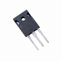
Mechanical Dimensions TO-247AB (FKS PKG CODE 001) FCH47N60F _F133 Rev. A. Dimensions in Millimeters 7 www.fairchildsemi.com ...

Page 8

... TRADEMARKS The following includes registered and unregistered trademarks and service marks, owned by Fairchild Semiconductor and/or its global subsidianries, and is not intended exhaustive list of all such trademarks. Build it Now™ CorePLUS™ CorePOWER™ CROSSVOLT™ CTL™ Current Transfer Logic™ ...

Related keywords