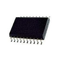
73S8014RN-IL/F Maxim Integrated Products, 73S8014RN-IL/F Datasheet - Page 15

73S8014RN-IL/F
Manufacturer Part Number
73S8014RN-IL/F
Description
IC SMART CARD 7816 EMV 20-SOIC
Manufacturer
Maxim Integrated Products
Datasheet
1.73S8014RN-DB.pdf
(28 pages)
Specifications of 73S8014RN-IL/F
Controller Type
Smart Card Interface
Voltage - Supply
2.7 V ~ 5.5 V
Operating Temperature
-40°C ~ 85°C
Mounting Type
Surface Mount
Package / Case
20-SOIC (0.300", 7.50mm Width) Exposed Pad
Lead Free Status / RoHS Status
Lead free / RoHS Compliant
Current - Supply
-
Interface
-
Lead Free Status / Rohs Status
Lead free / RoHS Compliant
Available stocks
Company
Part Number
Manufacturer
Quantity
Price
Company:
Part Number:
73S8014RN-IL/F
Manufacturer:
Maxim
Quantity:
234
Company:
Part Number:
73S8014RN-IL/F
Manufacturer:
TI
Quantity:
15
3.3 System Controller Interface
Three digital inputs allow direct control of the card interface by the host. The 73S8014RN is controlled as follows:
Interrupt output to the host: As long as the card is not activated, the OFF pin informs the host about the card
presence only (Low = No card in the reader). When CMDVCC is asserted low (Card activation sequence
requested from the host), low level on OFF means a fault has been detected (e.g. card removal during card
session, voltage fault, or over-current fault) that automatically initiates a deactivation sequence.
3.4 Power Supply and Voltage Supervision
The Teridian 73S8014RN smart card interface ICs incorporate a LDO voltage regulator for V
output is controlled by the digital input 5V/#V of the 73S8014RN. This regulator is able to provide either 3V or 5V
card voltage from the power supply applied on the V
65mA on
Digital circuitry is powered by the power supply applied on the VDD pin.
interface with the system controller. A card deactivation sequence is forced upon fault of any of this voltage
supervisor. One voltage supervisor constantly monitors the
sequencer at power-on, and to deactivate the card at power-off or upon fault. The voltage threshold of the
voltage supervisor is internally set by default to 2.26V nominal. However, it may be desirable, in some
applications, to modify this threshold value.
The method of adjusting the
supply and R1 from the VDDF_ADJ pin to ground (see application schematics). In order to set the new threshold
voltage, the equivalent voltage divider ratio must be determined. This ratio value will be designated Kx. Kx is
defined as R1/(R1+R3). Kx is calculated as:
Kx = (2.71 / V
To determine the values of R1 and R3, use the following formulas (the parallel resistance of R1 and R3 is
selected to be 24000 ohms)
R3 = 24000 / Kx
Taking the example above, where a V
Solving for R3 gives:
Solving for R1 gives:
Using standard 1 % resistor values gives R3 = 53.6KΩ and R1 = 43.2KΩ.
Using 1% external resistors and a parallel resistance of 24K ohms will result in a +/- 6% tolerance in the value of
VDD Fault. The sources of variation due to integrated circuit process variations and mismatches include the
internal reference voltage (less than +/- 1%), the internal comparator hysteresis and offset (less than +/- 1.7% for
part-to-part, processing and environment), the internal resistor value mismatch and value variations (less than
1.8%), and the external resistor values (1%).
If the 2.26V default threshold is used, this pin must be left unconnected.
Note: Since the V
voltage is greater than 4.85V before beginning a card session. In addition, VDD must be greater than the threshold
for VDD fault before card activation. Card activation begins on the falling edge of CMDVCC and therefore it must
be at VDD when the VDD and VPC supplies power up. When turning off power to the V
supplies, the card session should be terminated before shutdown or the V
4.85V when the VDD fault is detected and the emergency deactivation sequence is completed.
Rev. 1.0
Pin CMDVCC: When asserted low, starts an activation sequence
Pin RSTIN: controls the card RST signal (when enabled by the sequencer)
Pin 5V/#V: Defines the card
V
Kx = (2.71 / 2.6) - 0.595 = 0.4473.
CC
for both 3V and 5V that complies with EMV 4.0 and NDS specifications.
TH
) - 0.595 where V
DD
and the V
R1 = R3*(Kx / (1 – Kx))
R3 = 24000 / 0.4473 = 53654.
R1 = 58752 *(0.4473 / (1 – 0.4473)) = 43422.
V
DD
PC
V
fault voltage is to use a resistive network of R3 from the VDDF_ADJ pin to
power supplies are separate, special care must be taken to insure that the V
TH
DD
is the desired new threshold voltage.
voltage (5V when high and 3V when low)
DD
fault threshold voltage of 2.6V is desired, solving for Kx gives:
PC
pin. The voltage regulator can provide a current of at least
V
DD
voltage. It is used to initialize the ISO-7816-3
V
PC
DD
power supply must remain higher than
also defines the voltage range to
DD
and the V
CC
. The voltage
PC
power
V
V
DD
DD
PC
15


