ISL41334IRZ-T7A Intersil, ISL41334IRZ-T7A Datasheet - Page 17

ISL41334IRZ-T7A
Manufacturer Part Number
ISL41334IRZ-T7A
Description
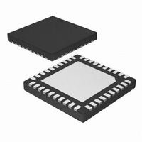
IC TXRX RS232/485 DL 2PRT 40QFN
Manufacturer
Intersil
Datasheet
1.ISL81334IAZ-T.pdf
(28 pages)
Specifications of ISL41334IRZ-T7A
Lead Free Status / RoHS Status
Lead free / RoHS Compliant
Available stocks
Company
Part Number
Manufacturer
Quantity
Price
Company:
Part Number:
ISL41334IRZ-T7A
Manufacturer:
Intersil
Quantity:
74
High ESD
All pins on the ISL81334, ISL41334 include ESD protection
structures rated at ±4kV (HBM), which is good enough to
survive ESD events commonly seen during manufacturing.
But the bus pins (Tx outputs and Rx inputs) are particularly
vulnerable to ESD events because they connect to an
exposed port on the exterior of the finished product. Simply
touching the port pins, or connecting a cable, can destroy an
unprotected port. ISL81334, ISL41334 bus pins are fitted
with advanced structures that deliver ESD protection in
excess of ±15kV (HBM), without interfering with any signal in
the RS-485 or the RS-232 range. This high level of
protection may eliminate the need for board level protection,
or at the very least will increase the robustness of any board
level scheme.
Small Packages
Many competing dual protocol ICs are available only in
monstrously large 24 to 28 Ld SOIC packages. The
ISL81334’s 28 Ld SSOP is 50% smaller than even a 24 Ld
SOIC, and the ISL41334’s tiny 6mmx6mm QFN is 80%
smaller than a 28 Ld SOIC.
Flow Through Pinouts
Even the ISL81334, ISL41334 pinouts are features, in that the
“flow-through” design simplifies board layout. Having the bus
pins all on one side of the package for easy routing to a cable
connector, and the Rx outputs and Tx inputs on the other side
for easy connection to a UART, avoids costly and problematic
crossovers. Figure 11 illustrates the flow-through nature of the
pinout.
Low Power Shutdown (SHDN) Mode
The ON/OFF pin is driven low to place the IC (both ports) in
the SHDN mode, and the already low supply current drops to
as low as 25µA. If this functionality isn’t desired, the pin can
be left disconnected (thanks to the internal pull-up), or it
should be connected to V
1kΩ resistor. SHDN disables the Tx and Rx outputs, and
disables the charge pumps if either port is in RS-232 mode,
so V+ collapses to V
FIGURE 11. ILLUSTRATION OF FLOW THROUGH PINOUT
A1
B1
Y1
Y2
B2
A2
Z1
Z2
CC
ISL81334
, and V- collapses to GND.
R
CC
D
17
(V
L
for the QFN), through a
RA1
DY1
DY2
RA2
µCONTROLLER
UART
ASIC
OR
OR
ISL81334, ISL41334
All but 5µA of SHDN I
LB, SP, DE) pull-up resistors (~20µA/resistor), so SHDN I
varies depending on the ISL81334, ISL41334 configuration.
The specification tables indicate the worst case values, but
careful selection of the configuration yields lower currents.
For example, in RS-232 mode the SP pins aren’t used, so if
both ports are configured for RS-232, floating or tying the SP
pins high minimizes SHDN I
the drivers are disabled in SHDN, so driving the DE pins
high during this time also reduces I
On the ISL41334, the SHDN I
V
V
input isn’t driven to the rail, so some I
Figure 21 for details.
When enabling from SHDN in RS-232 mode, allow at least
20µs for the charge pumps to stabilize before transmitting
data. The charge pumps aren’t used in RS-485 mode, so the
transceiver is ready to send or receive data in less than 1µs,
which is much faster than competing devices that require the
charge pump for all modes of operation.
Internal Loopback Mode
Driving the LB pin low places both ports in the loopback
mode, a mode that facilitates implementing board level self
test functions. In loopback, internal switches disconnect the
Rx inputs from the Rx outputs, and feed back the Tx outputs
to the appropriate Rx output. This way the data driven at the
Tx input appears at the corresponding Rx output (refer to
“Typical Operating Circuit” on page 6). The Tx outputs
remain connected to their terminals, so the external loads
are reflected in the loopback performance. This allows the
loopback function to potentially detect some common bus
faults such as one or both driver outputs shorted to GND, or
outputs shorted together.
Note that the loopback mode uses an additional set of
receivers, as shown in “Typical Operating Circuit” on page 6.
These loopback receivers are not standards compliant, so
the loopback mode can’t be used to implement a half-duplex
RS-485 transceiver.
If loopback won’t be utilized, the pin can be left disconnected
(thanks to the internal pull-up), or it should be connected to
V
ISL41334 (QFN Package) Special Features
Logic Supply (V
The ISL41334 (QFN) includes a V
inputs (Tx inputs and control pins) and Rx outputs. These
pins interface with “logic” devices such as UARTs, ASICs,
and µcontrollers, and today most of these devices use power
supplies significantly lower than 5V. Thus, a 5V output level
from a 5V powered dual protocol IC might seriously
overdrive and damage the logic device input. Similarly, the
L
CC
CC
powers the input stage and sets its V
. V
(V
CC
L
for the QFN), through a 1kΩ resistor.
powers the second stage, but the second stage
L
Pin)
CC
current is due to control input (ON,
CC
CC
. Likewise in RS-485 mode,
increases as V
L
CC
pin that powers the logic
CC
.
OH
current flows. See
at V
November 21, 2007
L
L
rather than
decreases.
FN6202.3
CC


