HV9921N3-G Supertex, HV9921N3-G Datasheet
HV9921N3-G
Specifications of HV9921N3-G


Related parts for HV9921N3-G


HV9921N3-G Summary of contents
Page 1
... HV9921. The peak current control scheme provides good regulation of the output current throughout the universal AC line voltage range 264VAC or DC input voltage 400V. VDD DRAIN HV9921 GND ● 1235 Bordeaux Drive, Sunnyvale, CA 94089 ) of approximately 10.5μs. OFF ● Tel: 408-222-8888 ● www.supertex.com HV9921 ...
Page 2
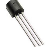
... OFF Note: * Denotes the specifications which apply over the full operating ambient temperature range of -40°C < Denotes guaranteed by design. Package Options TO-92 SOT-89 HV9921N3-G HV9921N8-G Pin Configurations Value -0.3 to +10V +5mA -40°C to +85°C -40° to +125°C -65° to +150°C ...
Page 3
... Bordeaux Drive, Sunnyvale, CA 94089 -40 - Junction Tem perature, °C 100 DRAIN Voltage 25° 125° DRAIN Voltage, V ● Tel: 408-222-8888 ● www.supertex.com HV9921 85 110 ...
Page 4
... Bordeaux Drive, Sunnyvale, CA 94089 4 is the current sense comparator threshold. The TH . Therefore, the initial output current accuracy might of the controller itself. These parasitic DRAIN )) L and lower junction capacitance DRAIN PCB L J ● Tel: 408-222-8888 ● www.supertex.com HV9921 and output PCB is the coil L (~10nF (3) ...
Page 5
... AC line voltage. The coefficients K AC can be determined from the minimum duty ratio of 0.7 0 0.3 0.2 0.1 0 0.1 0.2 0.3 0.4 Dm and K C Universal AC, 85-264VAC String of 10 LED (LW541C by OSRAM V = 4.1V max. each) F ● Tel: 408-222-8888 ● www.supertex.com HV9921 (9) (10) C 0.5 0.6 0.7 d ...
Page 6
... IN ECQ-E4104KF by Panasonic (0.1µF, 400V, IN LED ● Tel: 408-222-8888 ● www.supertex.com HV9921 41V ) − -LED 12 ...
Page 7
... VDD T = OFF 10.5µ REF - 300ns BLANK HV9921 ● 1235 Bordeaux Drive, Sunnyvale, CA 94089 7 DRAIN DRAIN ZERO VOLTAGE ZERO VOLTAGE TRANSITION TRANSITION DRAIN DRAIN DRAIN Regulator 7.5V R ● Tel: 408-222-8888 ● www.supertex.com HV9921 , Ch3 Ch3: I DRAIN DRAIN , Ch3 Ch3: I DRAIN DRAIN ...
Page 8
... D1 and the HV9921 together should IN be kept as small as possible. The switching loop area connecting the output filter capacitor C , the inductor L1 and the diode D1 together should be kept O as small as possible. Figure 7. Recommended circuit board layout with the HV9921N3 AC Line 85-264VAC Pin Description Pin # Function Description 1 DRAIN Drain terminal of the output switching MOSFET and a linear regulator input ...
Page 9
... Dimensions NOM - (inches) MAX .210 JEDEC Registration TO-92. * This dimension is not specified in the original JEDEC drawing. The value listed is for reference only. † This dimension is a non-JEDEC dimension. Drawings not to scale. Supertex Doc.#: DSPD-3TO92N3, Version D080408 Front View E E1 ...
Page 10
... Supertex inc. does not recommend the use of its products in life support applications, and will not knowingly sell them for use in such applications unless it receives an adequate “product liability indemnification insurance agreement.” Supertex inc. does not assume responsibility for use of devices described, and limits its liability to the replacement of the devices determined defective due to workmanship ...