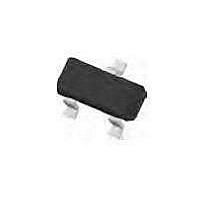
ZXLD381FHTA Diodes Inc, ZXLD381FHTA Datasheet - Page 4

ZXLD381FHTA
Manufacturer Part Number
ZXLD381FHTA
Description
LED Drivers SINGLE OR MULTI CELL
Manufacturer
Diodes Inc
Datasheet
1.ZXLD381FHTA.pdf
(9 pages)
Specifications of ZXLD381FHTA
Number Of Segments
1
Operating Supply Voltage
0.9 V to 2.2 V
Maximum Supply Current
20 mA
Maximum Power Dissipation
450 mW
Maximum Operating Temperature
+ 85 C
Mounting Style
SMD/SMT
Package / Case
SOT-23-3
Minimum Operating Temperature
0 C
Lead Free Status / RoHS Status
Lead free / RoHS Compliant
Lead Free Status / RoHS Status
Lead free / RoHS Compliant
Available stocks
Company
Part Number
Manufacturer
Quantity
Price
Company:
Part Number:
ZXLD381FHTA
Manufacturer:
PAM
Quantity:
12 000
A Product Line of
Diodes Incorporated
ZXLD381
Device Description
The ZXLD381 is a simple PFM, DC-DC controller combined with a high performance internal switching transistor, enabling the
production of a high efficiency boost converter for use in single cell applications. A block diagram is shown for the ZXLD381 in
Fig 1.
When power is applied, an oscillator within the pulse control block forces the internal switching transistor to switch on to start
an energy charge cycle. The low saturation voltage switch pulls the V
pin close to ground which forces the supply voltage
OUT
across the external inductor L1. This causes a current to build up, storing energy in the inductor. During this phase, switch
current and supply voltage are monitored and used by the pulse control circuit to determine the optimum drive conditions and
on-time. At the end of the energy charge cycle, the internal switch is turned off rapidly, interrupting the current flow through L1
which causes the voltage on V
to rise dramatically. When the voltage on V
reaches the load LED's forward (on)
OUT
OUT
voltage, the inductor current is transferred from the internal switch to the LED, starting the energy discharge cycle. With the
voltage across the inductor reversed, the current flowing through it (and the LED) now falls. When the inductor current reaches
zero, the voltage on the V
pin falls back towards V
. This action is sensed by the pulse control circuit, which initiates the
OUT
CC
next energy charge cycle. Except for low level losses, all the energy stored in the inductor during a charge cycle will be
channeled to the load LED during the following discharge cycle.
The current fed into the load LED has a sawtooth waveform, the average (DC) value of which is kept constant by the pulse
control circuit for varying supply voltage and temperature. It is possible to change the output current given by the ZXLD381 by
changing the value of inductor L1. The larger the inductance of L1, the lower the output current. A table/graph showing the
relationship between inductance and output current is given later in this datasheet. Since the output current of the ZXLD381 is
a sawtooth waveform, its peak value is substantially larger than the DC/average value. The table also provides this data.
The internal switching transistor has a minimum collector-emitter breakdown voltage of 20V and this sets the maximum load
voltage allowable. The minimum value is set by a feature of the pulse control circuit that requires the load voltage to be at least
0.8V greater than V
. (The device will function with load voltages smaller than this but output current regulation will be
CC
impaired.) Higher than nominal load voltages will lower the average (DC) output current generated for a given inductor value.
4 of 9
ZXLD381
May 2010
www.diodes.com
© Diodes Incorporated
Document number: DS32188 Rev. 3 - 2


