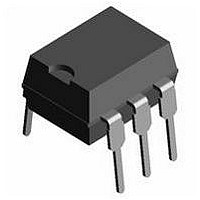
K3012P Vishay, K3012P Datasheet - Page 3

K3012P
Manufacturer Part Number
K3012P
Description
Triac & SCR Output Optocouplers Phototriac Output
Manufacturer
Vishay
Specifications of K3012P
Isolation Voltage
3750 Vrms
Configuration
1
Maximum Continuous Output Current
100 mA
Maximum Input Current
80 mA
Maximum Operating Temperature
+ 85 C
Maximum Power Dissipation
350 mW
Maximum Reverse Diode Voltage
5 V
Minimum Operating Temperature
- 40 C
Mounting Style
Through Hole
Output Type
AC
Package / Case
DIL
Typical Input Voltage
1.25 V
Zero-crossing Circuit
No
Output Device
Triac
Peak Output Voltage (vdrm)
250 V
Maximum Input Voltage
1.6 V
Maximum Output Voltage
175 VAC
Minimum Trigger Current
2 mA (Typ)
No. Of Channels
1
Optocoupler Output Type
Phototriac
Input Current
50mA
Output Voltage
250V
Opto Case Style
DIP
No. Of Pins
6
Mounting Type
Through Hole
Approval Bodies
UL, VDE
Blocking Voltage
250V
Rohs Compliant
Yes
Lead Free Status / RoHS Status
Lead free / RoHS Compliant
Lead Free Status / RoHS Status
Lead free / RoHS Compliant, Lead free / RoHS Compliant
Available stocks
Company
Part Number
Manufacturer
Quantity
Price
Note
(1)
Document Number: 83504
Rev. 2.0, 05-Mar-10
MAXIMUM SAFETY RATINGS
PARAMETER
INPUT
Forward current
OUTPUT
Power dissipation
COUPLER
Rated transient voltage
Safety temperature
Isolation test voltage
According to DIN EN60747-5-5 (see figure 4). This optocoupler is suitable for safe electrical isolation only within the safety ratings.
Compliance with the safety ratings shall be ensured by means of suitable protective circuits.
95 10814
+ 5 V
dV/dt
dV/dt
TT L
Optocoupler, Phototriac Output, 250 V
cr
crq
For technical questions, contact:
270
Highest value of the “rate of rise of off-state voltage” which does not cause any switching from the
off state to the on state
Highest value of the “rate of rise of communicating voltage” which does not switch on the device again,
after the voltage has decreased to zero and the trigger current is switched from I
TEST CONDITION
(1)
R
I
FT
S
I
I
F
F
Fig. 1 - Test Circuit for dV/dt
= 0
≥ I
Galvanic seperation
FT
Fig. 3 - Motor Control Circuit
P
SYMBOL
Fig. 2
dV/dt
S
I
S, INPUT
V
V
,
V
optocoupleranswers@vishay.com
IORM
IORM
OUTPUT
IOTM
T
si
95 10813
crq
0.1 µF
cr
and dV/dt
MIN.
R
L
K3010P, K3010PG Series
crq
DRM
V~
dV/dt
Vishay Semiconductors
TYP.
cr
M
FT
to zero
Test condition:
dV/dt
V
(sine wave)
R
dV/dt
V
(sine wave)
R
S
eff.
L
L
= 2/3 V
= 33 kΩ
= 2 kΩ
= 30 V
cr
crq
VAC ~
MAX.
DRM
95 10815
130
600
175
890
630
8
www.vishay.com
kV
UNIT
V
mW
mA
°C
RMS
V
peak
521


