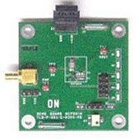
NCP5010EVB ON Semiconductor, NCP5010EVB Datasheet
NCP5010EVB
Specifications of NCP5010EVB


Related parts for NCP5010EVB

NCP5010EVB Summary of contents
Page 1
... The intent of the demo boards is to illustrate typical operation of the device for laboratory characterization. There are 2 demo boards offered, the NCP5010EVB which configures the device driving a string of 2−5 White LEDs in series. In this configuration the NCP5010 is operated in a ...
Page 2
... Current Selection: This jumper allows to select two different output current: Shorting jumper between J6−1 and J6−2 give a fixed output current determining by R1. Shorting jumper between J6−2 and J6−3 R3 allow adjusting the output current via potentiometer R3. NCP5010EVB/D Switch Descriptions Switch Descriptions http://onsemi.com ...
Page 3
... IOUT (mA) Figure 2. Efficiency vs. Current @ 2 LEDS ( IOUT (mA) Figure 4. Efficiency vs. Current @ 4 LEDS ( Figure 6. Ch1 SW, 5 V/div DC, Ch2 Vout, 5 V/div DC, Ch3 Vfb 100 mV/div DC, Ch4 Inductor Current 50 mA/div DC 200 ns/div NCP5010EVB 4 100 Figure 3. Efficiency vs. Current @ 3 LEDS (10 100 Figure 5. Efficiency vs. Current @ 5 LEDS (17 http://onsemi.com ...
Page 4
... PCB LAYOUT NCP5010EVB/D Figure 7. Assembly Layer Figure 8. Top Layer Routing http://onsemi.com 4 ...
Page 5
... L1 Resistor, chip Resistor, chip Adjustable Resistor, 100 TP1,TP2, Test point TP3 1 PCB PCB 2 2 1.0 mm, 4 Layer NCP5010EVB/D Size Manufacturer 8−Pin ON Semiconductor 1.7x1.7 mm Flip−Chip 0603 TDK 0805 TDK 1.2 x 2.2 mm OSRAM Weidmuller 0.200 x 4 Kontek Comatel Radiall 0.100 x 3 Std 3 ...
Page 6
... V CC TP4 Figure 9. Schematic Diagram for Demo Board NCP5010BIASEVB NCP5010EVB Then choose a standard value that is close to the above−calculated value. R2 should be 2 and R4 lower than 1 MW. The NCP5010 has built in short circuit protection so when . OUT the converter is started by a high logic signal on the CTRL pin a small current source (10 mA nominal) charges the (eq ...
Page 7
... To enable the boost converter connect a shorting jumper between J4−1 and J4−2 J3 Voltage Selection: This jumper allows to select two different output voltage: Shorting jumper between J6−2 and J6−3 give a fixed output voltage setup by R2/R4. Shorting jumper between J6−1 and J6−2 R3 allow adjusting the output voltage. NCP5010EVB/D Switch Descriptions Switch Descriptions http://onsemi.com 7 ...
Page 8
... IOUT (mA) Figure 12. Efficiency vs mH, VLF 4012−100 V OUT 4 3 IOUT (mA) Figure 14. Efficiency vs mH, VLF 4012−100 V OUT NCP5010EVB/D Figure 11. Efficiency vs. I OUT = 6 mH, VLF 4012−220 V OUT 3 100 Figure 13. Efficiency vs. I OUT = mH, VLF 4012−220 V OUT 3 100 1 Figure 15. Efficiency vs. I OUT = mH, VLF 4012− ...
Page 9
... TYPICAL OPERATING CHARACTERISTICS Figure 16. Load Transient Response 2V/div DC, 3 IOUT, 10mA/div DC ms/div OUT Figure 18. Line Transient Rejection 5V/div DC, 3 VOUT, 50mV/div AC ms/div OUT NCP5010EVB/D 100 10 1 0.10 0. Figure 17. Output Switching Noise V OUT = VLF 4012−220 V OUT 3 http://onsemi.com 9 100 ...
Page 10
... PCB LAYOUT NCP5010EVB/D Figure 19. Assembly Layer Figure 20. Top Layer Routing http://onsemi.com 10 ...
Page 11
... C1608X5R0J475MT GRM21BR61E475KA or C2012X5R1C475MT SL5.08/2/90B + BLZ 5.08/2 4711955140470 Std VLF4012AT−220MR51 Std Std 3224W −1− 504 − Std TLS−P−002−B−0304−HG ON Semiconductor Website: www.onsemi.com Order Literature: http://www.onsemi.com/orderlit For additional information, please contact your local Sales Representative NCP5010EVB/D ...