AVR-GSM Olimex Ltd., AVR-GSM Datasheet - Page 15
AVR-GSM
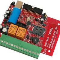
Manufacturer Part Number
AVR-GSM
Description
MCU, MPU & DSP Development Tools DEV BRD FOR ATMEGA32 32KB FLASH 2KB RAM
Manufacturer
Olimex Ltd.
Datasheet
1.AVR-GSM.pdf
(22 pages)
Specifications of AVR-GSM
Processor To Be Evaluated
ATMega32
Data Bus Width
8 bit
Interface Type
USB, SPI, UART
Dimensions
130 mm x 82 mm
Operating Supply Voltage
12 V
Tool Type
Development Kit
Core Architecture
AVR
Cpu Core
AVR 8
Silicon Manufacturer
Atmel
Silicon Core Number
ATmega32
Kit Contents
Board
Features
USB Interface, On-Board Temperature Digital Sensor
Rohs Compliant
Yes
Lead Free Status / RoHS Status
Lead free / RoHS Compliant
Other names
1776311 52R3434


EXT is connector for external plug-in modules. It's standard 26 pin ribbon cable IDC keyed
connector.
Backup: RTC backup power supply for the GSM module real time clock and RAM, when the
battery is discharged. If the battery attached to this signal is chargeable and the voltage
level is low the module will charge the battery. Vnom = 1.8V, Inom= 20uA
AREF: Analog reference input of ATMega32 microcontroller. Can be used for external
analogue circuits.
GND: Digital ground.
3VA: Analog power supply of ATMega32 microcontroller. This is 3VDC output which can be
used for external analog modules.
3V: Digital power of ATMega32. This is 3VDC output for external digital modules.
AGND: Analog ground of ATMega32 microcontroller. Can be used for external analog
circuits.
VBAT: Dedicated to connect main Li-ion battery. The power supply of GSM module has to
be a single voltage source of VBAT= 3.4V...4.5V. Li-ion battery with 650mA capacity is used
in AVR-GSM.
ADC3/PA3: ADC3 input/digital IO of ATMega32.
+5V: +5VDC output / up to 2A current source
POWERKEY: This is GSM module power on/off key. When the module is ON if you press
and hold for more than 3 seconds the module go in power down state. If the module if in
power down mode and you press and hold this key for more than 1 second the module will
go in ON mode.
ADC1/PA1: ADC1 input/digital IO of ATMega32.
AUXADC: This is general purpose analog to digital converter build-in the GSM module. The
input voltage value should be in range 0V to 2.4V. This pin value can be read with AT
command.
ADC0/PA0: ADC0 input/digital IO of ATMega32.
GPO1: This is GPO of GSM module and can be configured by AT command for outputting
high or low level voltage. All of the GPOs are initialy in low state without any setting from AT
command.
(SCK)PB7,(MISO)PB6,(MOSI)PB5,(SS)PB4: ATMega32 SPI pins.
SPI_DATA,SPI_CLK,SPI_CS,SPI_D/C: This is GSM module SPI port reserved for future use.
KBROW0: This is external keyboard input pin of GSM module.
RST: ATMega32 Reset pin. Open collector output.
Page 15
Related parts for AVR-GSM
Image
Part Number
Description
Manufacturer
Datasheet
Request
R

Part Number:
Description:
MCU, MPU & DSP Development Tools PROTOTYPE BRD FOR STK200 20PIN
Manufacturer:
Olimex Ltd.
Datasheet:

Part Number:
Description:
MCU, MPU & DSP Development Tools PROTOTYPE BRD FOR STK200 28PIN
Manufacturer:
Olimex Ltd.
Datasheet:

Part Number:
Description:
MCU, MPU & DSP Development Tools PROTOTYPE BRD FOR STK200 10PIN
Manufacturer:
Olimex Ltd.
Datasheet:

Part Number:
Description:
Programmers & Debuggers AVR PROGRAMMER 2MB FLASH
Manufacturer:
Olimex Ltd.
Datasheet:

Part Number:
Description:
MCU, MPU & DSP Development Tools PROTOTYPE BRD FOR AT90USB162
Manufacturer:
Olimex Ltd.
Datasheet:

Part Number:
Description:
Programmers & Debuggers AVR PROGRAMMER 2MB FLASH 1000V
Manufacturer:
Olimex Ltd.
Datasheet:

Part Number:
Description:
Programmers & Debuggers USB AVR PROGRAMMER
Manufacturer:
Olimex Ltd.
Datasheet:

Part Number:
Description:
MCU, MPU & DSP Development Tools DEV BRD FOR AT90CAN128
Manufacturer:
Olimex Ltd.
Datasheet:

Part Number:
Description:
MCU, MPU & DSP Development Tools HDR BRD FOR AT90CAN128-16AU
Manufacturer:
Olimex Ltd.
Datasheet:

Part Number:
Description:
MCU, MPU & DSP Development Tools DEV BRD FOR AT90USB162
Manufacturer:
Olimex Ltd.
Datasheet:

Part Number:
Description:
Microcontroller & Microprocessor Development Tools TCP-IP DEV BRD PIC32MX460F512
Manufacturer:
Olimex Ltd.
Datasheet:

Part Number:
Description:
Microcontroller & Microprocessor Development Tools PROTOTYPE BOARD TMS320F28027
Manufacturer:
Olimex Ltd.
Datasheet:

Part Number:
Description:
Microcontroller & Microprocessor Development Tools HDR BRD FOR LPC3131
Manufacturer:
Olimex Ltd.
Datasheet:

Part Number:
Description:
Microcontroller & Microprocessor Development Tools MP3 PLYR MOD WITH VS1002
Manufacturer:
Olimex Ltd.
Datasheet:
Part Number:
Description:
Microcontroller & Microprocessor Development Tools MP3 PLYR MOD BAT WITH VS1002
Manufacturer:
Olimex Ltd.
Datasheet: