DR3000 RFM, DR3000 Datasheet - Page 3
DR3000
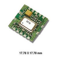
Manufacturer Part Number
DR3000
Description
RF Modules & Development Tools Transceiver Module 2G, 916.5MHz 2.4kbps
Manufacturer
RFM
Datasheet
1.DR3000.pdf
(5 pages)
Specifications of DR3000
Lead Free Status / RoHS Status
Lead free / RoHS Compliant


Pin Descriptions
www.RFM.com
©2008 by RF Monolithics, Inc.
Pin
1
2
3
4
5
6
7
AGC/VCC
RX DATA
RX BBO
PK DET
Name
TX IN
GND
GND
E-mail: info@rfm.com
This pin is connected directly to the transceiver AGCCAP pin. To disable AGC operation, this pin is tied to VCC. To enable AGC
operation, a capacitor is placed between this pin and ground. This pin controls the AGC reset operation. A capacitor between
this pin and ground sets the minimum time the AGC will hold-in once it is engaged. The hold-in time is set to avoid AGC chat-
tering. For a given hold-in time t
C
A ±10% ceramic capacitor should be used at this pin. The value of C
2.65* t
longest run of zero bits that can occur in a received data stream. The AGC hold-in time can be greater than the peak detector
decay time, as discussed below. However, the AGC hold-in time should not be set too long, or the receiver will be slow in
returning to full sensitivity once the AGC is engaged by noise or interference. The use of AGC is optional when using OOK
modulation with data pulses of at least 30 µs. Active or latched AGC operation is required for ASK modulation and/or for data
pulses of less than 30 µs. The AGC can be latched ON once engaged by connecting a 150 K resistor between this pin and
ground, instead of a capacitor. AGC operation depends on a functioning peak detector, as discussed below. The AGC capacitor
is discharged in the transceiver power-down (sleep) mode and in the transmit modes. Note that provisions are made on the cir-
cuit board to install a jumper between this pin and the junction of C2 and L3. Installing the jumper allows either this pin or Pin 7
to be used for the Vcc supply when AGC operation is not required.
This pin is connected directly to the transceiver PKDET pin. This pin controls the peak detector operation. A capacitor between
this pin and ground sets the peak detector attack and decay times, which have a fixed 1:1000 ratio. For most applications, the
attack time constant should be set to 6.4 ms with a 0.027 µF capacitor to ground. (This matches the peak detector decay time
constant to the time constant of the 0.1 µF coupling capacitor C3.) A ±10% ceramic capacitor should be used at this pin. The
peak detector is used to drive the “dB-below-peak” data slicer and the AGC release function. The AGC hold-in time can be
extended beyond the peak detector decay time with the AGC capacitor, as discussed above. Where low data rates and OOK
modulation are used, the “dB-below-peak” data slicer and the AGC are optional. In this case, the PKDET pin can be left uncon-
nected, and the AGC pin can be connected to VCC to reduce the number of external components needed. The peak detector
capacitor is discharged in the transceiver power-down (sleep) mode and in the transmit modes. See the description of Pin 3
below for further information.
This pin is connected directly to the transceiver BBOUT pin. On the circuit board, BBOUT also drives the transceiver CMPIN
pin through C3, a 0.1 µF coupling capacitor (t
cess (DSP, etc.). The nominal output impedance of this pin is 1 K. The RX BBO signal changes about 10 mV/dB, with a peak-
to-peak signal level of up to 675 mV. The signal at RX BBO is riding on a 1.1 Vdc value that varies somewhat with supply volt-
age and temperature, so it should be coupled through a capacitor to an external load. A load impedance of 50 K to 500 K in
parallel with no more than 10 pF is recommended. Note the AGC reset function is driven by the signal applied to CMPIN
through C3. When the transceiver is in power-down (sleep) or in a transmit mode, the output impedance of this pin becomes
very high, preserving the charge on the coupling capacitor(s). The value of C3 on the circuit board has been chosen to match
typical data encoding schemes at 2.4 kbps. If C3 is modified to support higher data rates and/or different data encoding
schemes and PK DET is being used, make the value of the peak detector capacitor about 1/3 the value of C3.
RX DATA is connected directly to the transceiver data output pin, RXDATA. This pin will drive a 10 pF, 500 K parallel load. The
peak current available from this pin increases with the receiver low-pass filter cutoff frequency. In the power-down (sleep) or
transmit modes, this pin becomes high impedance. If required, a 1000 K pull-up or pull-down resistor can be used to establish
a definite logic state when this pin is high impedance (do not connect the pull-up resistor to a supply voltage higher than 3.5
Vdc or the transceiver will be damaged). This pin must be buffered to successfully drive low-impedance loads.
The TX IN pin is connected to the transceiver TXMOD pin through a 4.7 K resistor on the circuit board. Additional series resis-
tance will often be required between the modulation source and the TX IN pin, depending on the desired output power and
peak modulation voltage (3.3 K typical for a peak modulation voltage of 3 volts). Saturated output power requires about 450 µA
of drive current. Peak output power PO for a 3 Vdc supply is approximately:
PO = 4.8*((V
resistor R
This pin must be held low in the receive and sleep modes. Please refer to section 2.9 of the ASH Transceiver Designer’s Guide
for additional information.
This is a ground pin.
This is a ground pin.
AGC
= 19.1* t
AGH
M
, depending on operating voltage, temperature, etc. The hold-in time is chosen to allow the AGC to ride through the
is in kilohms
TXH
AGH
– 0.9)/(R
, where t
M
AGH
+ 4.7))
AGH
is in µs and C
2
, the capacitor value C
, where P
BBC
O
AGC
is in mW, peak modulation voltage V
= 6.4 ms). RX BBO can also be used to drive an external data recovery pro-
is in pF
Description
AGC
is:
AGC
given above provides a hold-in time between t
TXH
is in volts and external modulation
DR3000 - 4/8/08
AGH
Page 3 of 5
and
Related parts for DR3000
Image
Part Number
Description
Manufacturer
Datasheet
Request
R

Part Number:
Description:
RF Modules & Development Tools TRC105 Evaluation Board 447-451 MHz
Manufacturer:
RFM
Datasheet:
Part Number:
Description:
RF Modules & Development Tools TRC105 Evaluation Board 365-381 MHz
Manufacturer:
RFM
Datasheet:
Part Number:
Description:
RF Modules & Development Tools TRC105 Evaluation Board 303-307 MHz
Manufacturer:
RFM
Datasheet:
Part Number:
Description:
RF Modules & Development Tools TRC105 Evaluation Board 382-398 MHz
Manufacturer:
RFM
Datasheet:
Part Number:
Description:
RF Modules & Development Tools TRC105 Evaluation Board 416-436 MHz
Manufacturer:
RFM
Datasheet:
Part Number:
Description:
RF Modules & Development Tools TRC105 Evaluation Board 342-348 MHz
Manufacturer:
RFM
Datasheet:
Part Number:
Description:
RF Modules & Development Tools TRC105 Evaluation Board 402-407 MHz
Manufacturer:
RFM
Datasheet:
Part Number:
Description:
RF Modules & Development Tools TRC105 Evaluation Board 310-319 MHz
Manufacturer:
RFM
Datasheet:

Part Number:
Description:
RF Modules & Development Tools TXC101 Development Kit 310-319 MHz
Manufacturer:
RFM
Part Number:
Description:
RF Modules & Development Tools TXC102 Development Kit 430-439 MHz
Manufacturer:
RFM


Part Number:
Description:
10-Terminal Ceramic Surface-Mount Case 7 x 5 mm Nominal Footprint
Manufacturer:
RFM [RF Monolithics, Inc]
Datasheet:
Part Number:
Description:
QUAD-BAND GSM850/GSM/DCS/PCS POWER AMP MODULE
Manufacturer:
RFM [RF Monolithics, Inc]
Datasheet:
Part Number:
Description:
402 to 405 MHz Medical Band Front-end Filter
Manufacturer:
RFM [RF Monolithics, Inc]
Datasheet:
Part Number:
Description:
674.03 MHz SAW Resonator
Manufacturer:
RFM [RF Monolithics, Inc]
Datasheet: