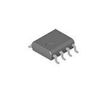
AH322-S8PCB900 TriQuint, AH322-S8PCB900 Datasheet - Page 2

AH322-S8PCB900
Manufacturer Part Number
AH322-S8PCB900
Description
RF Modules & Development Tools 400-2700MHz Eval Board
Manufacturer
TriQuint
Datasheet
1.AH322-S8PCB2140.pdf
(8 pages)
Specifications of AH322-S8PCB900
Board Size
6.2 mm x 5 mm x 1.62 mm
Minimum Frequency
400 MHz
Minimum Operating Temperature
- 40 C
Supply Voltage (min)
5 V
Product
RF Modules
Maximum Frequency
2.7 GHz
Output Power
2 W
Supply Voltage (max)
8 V
Supply Current
1400 mA
Maximum Operating Temperature
+ 85 C
For Use With/related Products
AH322
Lead Free Status / RoHS Status
Lead free / RoHS Compliant
Other names
1071300
TriQuint Semiconductor, Inc • Phone 1-800-951-4401 • FAX: 408-577-6633 • e-mail: info-sales@tqs.com • Web site: www.TriQuint.com
AH322
2W High Linearity InGaP HBT Amplifier
45
40
35
30
25
20
15
10
-5
5
0
0
Notes:
S-Parameters (V
The gain for the unmatched device in 50 ohm system is shown as the trace in pink color, [DB (S (2, 1)]. For a tuned circuit for a
particular frequency, it is expected that actual gain will be higher, up to the maximum stable gain. The maximum stable gain is shown in
the blue line [DB (GMAX)].
The impedance plots are shown from 0.01 – 4 GHz, with markers placed in 0.5 GHz increments.
Freq (MHz)
0.5
1000
1200
1400
1600
1800
2000
2200
2400
2600
2800
3000
100
200
400
600
700
800
DB(MSG())
De_emebedded S_parameter
50
Gain and Maximum Stable Gain
Circuit Board Material: Top RF layer is .014” Getek,
1 oz copper, Microstrip line details: width = .026”, spacing = .026”
The silk screen markers ‘A’, ‘B’, ‘C’, etc. and ‘1’, ‘2’, ‘3’, etc. are used as placemarkers for the input and output tuning
shunt capacitors – C8, C5 and C2. The markers and vias are spaced in .050” increments.
1
2.14 GHz
7.19 dB
Frequency (GHz)
cc
= +5 V, I
S11 (dB)
-0.74
-0.53
-0.45
-0.44
-0.56
-0.61
-0.64
-0.78
-0.87
-1.08
-1.94
-5.84
-6.52
-4.45
-2.44
-1.26
-1.4
-3.2
1.5
cq
S-Parameters (Vcc = +5 V, I
DB(|S(2,1)|)
De_emebedded S_parameter
= 500 mA, T = 25 °C, unmatched 50 ohm system, calibrated to device leads)
Application Circuit PC Board Layout
2
S11 (ang)
-174.58
-179.31
176.71
170.07
163.11
156.03
147.66
138.49
128.32
117.39
106.19
112.96
121.06
117.78
108.49
159.9
94.01
95.9
2.14 GHz
22.7 dB
2.5
Typical Device Data
S21 (dB)
3
29.75
24.21
18.46
12.77
-1.12
9.78
8.73
7.94
6.11
5.83
6.17
7.36
4.77
2.24
6.8
5.8
6.8
6.5
cq
= 500 mA, T = 25 °C, calibrated to device leads)
S21 (ang)
є
-121.06
-142.85
109.51
-33.75
-64.88
-92.83
r
98.59
89.55
80.82
73.71
69.49
65.68
56.95
46.99
36.79
25.05
10.83
-7.89
= 4.0, 4 total layers (0.062” thick) for mechanical rigidity
S11
S12 (dB)
-43.47
-43.22
-42.49
-42.04
-41.41
-41.21
-40.26
-39.65
-38.34
-37.99
-37.52
-37.39
-37.45
-38.56
-41.93
-41.83
-38.13
-34.99
2.14 GHz
r 0.493722
x 0.825153
Swp Max
Swp Min
0.01GHz
S12 (ang)
4GHz
-115.31
167.17
103.07
-14.57
-27.07
-42.22
-69.38
25.51
17.83
8.135
10.52
11.31
62.15
5.31
12.5
7.88
2.45
-3.1
S22 (dB)
-1.15
-1.22
-1.19
-1.22
-1.18
-1.12
-1.17
-1.22
-1.26
-1.33
-1.49
-1.46
-1.41
-1.21
-0.27
-0.35
-0.9
-0.4
2.14 GHz
r 0.0838672
x 0.36526
S22
S22 (ang)
-157.31
-178.39
176.07
173.93
171.69
166.82
162.15
157.29
152.31
147.31
143.05
133.24
126.56
119.41
112.36
-135.3
-170.3
138.4
Swp Max
Swp Min
0.01GHz
4GHz
April 2009
.


