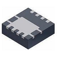
FDMC3020DC Fairchild Semiconductor, FDMC3020DC Datasheet - Page 2

FDMC3020DC
Manufacturer Part Number
FDMC3020DC
Description
MOSFET Power 30V NChan Dual Cool PowerTrench SyncFET
Manufacturer
Fairchild Semiconductor
Datasheet
1.FDMC3020DC.pdf
(8 pages)
Specifications of FDMC3020DC
Gate Charge Qg
15.5 nC
Minimum Operating Temperature
- 55 C
Configuration
Dual
Transistor Polarity
N-Channel
Resistance Drain-source Rds (on)
5 mOhms
Forward Transconductance Gfs (max / Min)
44 S
Drain-source Breakdown Voltage
30 V
Gate-source Breakdown Voltage
20 V
Continuous Drain Current
17 A
Power Dissipation
3 W
Maximum Operating Temperature
+ 150 C
Mounting Style
SMD/SMT
Package / Case
Power 33
Lead Free Status / RoHS Status
Lead free / RoHS Compliant
Available stocks
Company
Part Number
Manufacturer
Quantity
Price
Part Number:
FDMC3020DC
Manufacturer:
FAIRCHILD/ن»™ç«¥
Quantity:
20 000
©2010 Fairchild Semiconductor Corporation
FDMC3020DC Rev.C3
Electrical Characteristics
Off Characteristics
On Characteristics
Dynamic Characteristics
Switching Characteristics
Drain-Source Diode Characteristics
BV
ΔBV
I
I
V
r
g
C
C
C
R
t
t
t
t
Q
Q
Q
Q
V
t
Q
ΔV
DSS
GSS
d(on)
r
d(off)
f
rr
DS(on)
FS
GS(th)
SD
iss
oss
rss
g
ΔT
ΔT
g
g
gs
gd
rr
Symbol
DSS
GS(th)
DSS
J
J
Drain to Source Breakdown Voltage
Breakdown Voltage Temperature
Coefficient
Zero Gate Voltage Drain Current
Gate to Source Leakage Current
Gate to Source Threshold Voltage
Gate to Source Threshold Voltage
Temperature Coefficient
Static Drain to Source On Resistance
Forward Transconductance
Input Capacitance
Output Capacitance
Reverse Transfer Capacitance
Gate Resistance
Turn-On Delay Time
Rise Time
Turn-Off Delay Time
Fall Time
Total Gate Charge
Total Gate Charge
Gate to Source Gate Charge
Gate to Drain “Miller” Charge
Source to Drain Diode Forward Voltage
Reverse Recovery Time
Reverse Recovery Charge
Parameter
T
J
= 25 °C unless otherwise noted
V
V
V
V
V
f = 1 MHz
V
I
V
V
V
V
V
V
I
I
I
V
V
D
F
D
D
DD
GS
GS
GS
GS
GS
GS
GS
DS
DS
GS
GS
DS
GS
= 12 A, di/dt = 100 A/μs
= 250 μA, referenced to 25 °C
= 250 μA, V
= 250 μA, referenced to 25 °C
= 15 V, V
= 15 V, I
= 10 V, R
= 0 V to 10 V
= 0 V to 4.5 V
= 5 V, I
= 0 V, I
= 0 V, I
= 24 V, V
= V
= 10 V, I
= 4.5 V, I
= 10 V, I
= ±20 V, V
2
DS
Test Conditions
, I
D
S
S
D
D
D
D
= 1.9 A
D
= 12 A
= 12 A
GS
GEN
GS
= 250 μA
GS
= 12 A,
= 12 A
= 12 A, T
DS
= 10 A
= 0 V,
= 0 V
= 0 V
= 0 V
= 6 Ω
V
I
D
DD
= 12 A
J
= 15 V,
(Note 2)
= 125 °C
(Note 2)
Min
1.0
30
1038
0.82
0.73
513
15.5
0.9
Typ
1.9
5.0
7.2
7.5
87
7.1
2.5
25
44
19
-6
9
17
9
3
2
3
1385
±100
6.25
Max
685
135
10.6
1.3
1.2
3.0
9.0
9.1
45
18
18
10
35
10
23
www.fairchildsemi.com
1
mV/°C
mV/°C
Units
mΩ
nC
pF
pF
pF
μA
nA
nC
nC
nC
nC
ns
Ω
ns
ns
ns
ns
V
V
S
V


