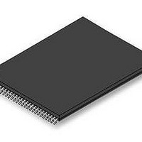
S29GL128P11TFI020 Spansion Inc., S29GL128P11TFI020 Datasheet - Page 21

S29GL128P11TFI020
Manufacturer Part Number
S29GL128P11TFI020
Description
Flash 3V 128Mb Mirrorbit lowest address110ns
Manufacturer
Spansion Inc.
Specifications of S29GL128P11TFI020
Memory Type
NOR
Memory Size
128 Mbit
Access Time
110 ns
Data Bus Width
8 bit, 16 bit
Architecture
Sectored
Interface Type
Serial
Supply Voltage (max)
3.6 V
Supply Voltage (min)
2.7 V
Maximum Operating Current
50 mA
Mounting Style
SMD/SMT
Operating Temperature
+ 85 C
Package / Case
TSOP-56
Memory Configuration
128K X 16
Ic Interface Type
Parallel
Supply Voltage Range
2.7V To 3.6V
Memory Case Style
TSOP
No. Of Pins
56
Lead Free Status / RoHS Status
Lead free / RoHS Compliant
Lead Free Status / RoHS Status
Lead free / RoHS Compliant, Lead free / RoHS Compliant
Available stocks
Company
Part Number
Manufacturer
Quantity
Price
Company:
Part Number:
S29GL128P11TFI020
Manufacturer:
SPANSION
Quantity:
1 133
Part Number:
S29GL128P11TFI020
Manufacturer:
SPANSION
Quantity:
20 000
7.7
November 21, 2006 S29GL-P_00_A3
7.7.1
Program/Erase Operations
Single Word Programming
These devices are capable of several modes of programming and or erase operations which are described in
detail in the following sections.
During a write operation, the system must drive CE# and WE# to V
address, command, and data. Addresses are latched on the last falling edge of WE# or CE#, while data is
latched on the 1st rising edge of WE# or CE#.
The Unlock Bypass feature allows the host system to send program commands to the Flash device without
first writing unlock cycles within the command sequence. See
function.
Note the following:
Single word programming mode is one method of programming the Flash. In this mode, four Flash command
write cycles are used to program an individual Flash address. The data for this programming operation could
be 8 or 16-bits wide.
While the single word programming method is supported by all Spansion devices, in general it is not
recommended for devices that support Write Buffer Programming. See
required bus cycles and
When the Embedded Program algorithm is complete, the device then returns to the read mode and
addresses are no longer latched. The system can determine the status of the program operation by using
DQ7 or DQ6. Refer to the Write Operation Status section for information on these status bits.
When the Embedded Program algorithm is complete, the device returns to the read mode.
The system can determine the status of the program operation by using DQ7 or DQ6. Refer to the Write
Operation Stat section for information on these status bits.
An “0” cannot be programmed back to a “1.” A succeeding read shows that the data is still “0.”
Only erase operations can convert a “0” to a “1.”
Any commands written to the device during the Embedded Program Algorithm are ignored except the
Program Suspend command.
Secured Silicon Sector, Autoselect, and CFI functions are unavailable when a program operation is in
progress.
A hardware reset immediately terminates the program operation and the program command sequence
should be reinitiated once the device has returned to the read mode, to ensure data integrity.
Programming is allowed in any sequence and across sector boundaries for single word programming
operation.
Programming to the same word address multiple times without intervening erases is permitted.
During programming, any command (except the Suspend Program command) is ignored.
The Secured Silicon Sector, Autoselect, and CFI functions are unavailable when a program operation is in
progress.
A hardware reset immediately terminates the program operation. The program command sequence should
be reinitiated once the device has returned to the read mode, to ensure data integrity.
Programming to the same address multiple times continuously (for example, “walking” a bit within a word)
is permitted.
D a t a
S h e e t
Figure 7.1
( A d v a n c e
S29GL-P MirrorBit
for the flowchart.
I n f o r m a t i o n )
TM
Flash Family
Section 7.7.8
IL
and OE# to VIH when providing an
Table 12.1 on page 61
for details on the Unlock Bypass
for the
19


