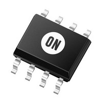
NCP3126ADR2G ON Semiconductor, NCP3126ADR2G Datasheet - Page 18

NCP3126ADR2G
Manufacturer Part Number
NCP3126ADR2G
Description
DC/DC Switching Converters 3A PWM Switching Buck Regulator
Manufacturer
ON Semiconductor
Datasheet
1.NCP3126ADR2G.pdf
(23 pages)
Specifications of NCP3126ADR2G
Mounting Style
SMD/SMT
Duty Cycle (max)
80 %
Efficiency
93 %
Input / Supply Voltage (max)
13.2 V
Input / Supply Voltage (min)
4.5 V
Maximum Operating Temperature
+ 125 C
Minimum Operating Temperature
- 40 C
Operating Temperature Range
- 40 C to + 125 C
Output Current
3 A
Output Voltage
Adjustable
Supply Current
10 mA
Switching Frequency
350 KHz
Package / Case
SOIC-8
Lead Free Status / RoHS Status
Lead free / RoHS Compliant
Available stocks
Company
Part Number
Manufacturer
Quantity
Price
Company:
Part Number:
NCP3126ADR2G
Manufacturer:
ON
Quantity:
2 500
22 mF with a crossover frequency of 35 kHz, the
compensation values for common output voltages can be
calculated as shown in Table 6:
Calculating Soft−Start Time
following equations can be used.
C
C
I
a regulated output voltage is t
SS
Table 6. COMPENSATION VALUES
P
C
Assuming an output capacitance of 470 mF in parallel with
To calculate the soft−start delay and soft−start time, the
The time the output voltage takes to increase from 0 V to
V
(V)
12
12
12
12
12
12
12
12
12
t
t
5
5
5
5
5
5
5
in
SSdelay
SS
7.45 ms +
2.51 ms +
+
C
V
+
0.8
1.0
1.1
1.2
1.5
1.8
2.5
3.3
5.0
0.8
1.0
1.1
1.2
1.5
1.8
2.5
(V)
out
P
) C
= Compensation pole capacitor
= Compensation capacitor
= Soft−start current
C
P
2.83 nF ) 80 nF
2.83 nF ) 80 nF
) C
C
L
(mF)
3.3
3.3
3.3
4.7
4.7
6.8
6.8
8.2
3.3
3.3
3.3
4.7
4.7
4.7
4.7
10
I
out
SS
I
C
SS
D
10 mA
0.180
0.180
0.180
0.180
0.180
0.220
0.220
0.220
0.180
0.180
0.180
0.180
0.180
0.180
(nF)
0.9 V
Cf
V
NI
NI
ss
ramp
10 mA
as shown in Equation 46:
³
(nF)
180
120
120
120
120
100
100
100
100
100
Cc
82
82
82
82
82
82
0.9 V
27.5%
0.357
0.442
0.475
0.787
0.909
0.887
(kW)
1.87
2.05
1.65
1.82
2.21
2.61
1.5
2.5
1.1
3.4
Rc
1.1 V
(eq. 45)
(eq. 46)
http://onsemi.com
(nF)
0.82
0.82
0.82
0.82
0.82
2.7
2.7
2.2
2.2
1.8
1.2
1.2
1.8
1.5
Cp
1
1
18
C
C
D
I
t
V
to the bottom of the ramp is considered t
delay time is the addition of the current set delay and t
which in this case is 9 ms and 7.45 ms respectively, for a
total of 16.45 ms.
Calculating Input Inrush Current
charging and output charging. The input charging of a buck
stage is usually not controlled, and is limited only by the
input RC network, and the output impedance of the upstream
power stage. If the upstream power stage is a perfect voltage
source, then the input charge inrush current can be depicted
as shown in Figure 26 and calculated as:
SS
SS
P
C
ramp
The delay from the charging of the compensation network
The input inrush current has two distinct stages: input
Figure 26. Input Charge Inrush Current
Vcomp
Vout
I
ICinrush_PK
120 A +
IPK
= Compensation pole capacitor
= Compensation capacitor
= Duty ratio
= Soft−start interval
= Peak−to−peak voltage of the ramp
= Soft−start current
Figure 25. Soft−Start Ramp
1 +
0.1
12
CIN
V
V
IN
ESR
900 mV
ssdelay
. The total
(eq. 47)
ssdelay
,


