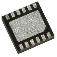
MD1213K6-G Supertex, MD1213K6-G Datasheet - Page 3

MD1213K6-G
Manufacturer Part Number
MD1213K6-G
Description
MOSFET & Power Driver ICs HI SPD DUAL MOSFET DRIVER
Manufacturer
Supertex
Type
High Side/Low Sider
Datasheet
1.MD1213K6-G.pdf
(7 pages)
Specifications of MD1213K6-G
Rise Time
6 ns
Fall Time
6 ns
Supply Voltage (min)
4.5 V
Supply Current
6.6 mA
Maximum Operating Temperature
+ 85 C
Mounting Style
SMD/SMT
Minimum Operating Temperature
- 20 C
Number Of Drivers
2
Number Of Outputs
2
Package / Case
QFN-12
Lead Free Status / RoHS Status
Lead free / RoHS Compliant
Logic Truth Table
DC Electrical Characteristics
(Over operating conditions unless otherwise specified, V
Outputs
AC Electrical Characteristics
l t
R
PLH
I
l t
Sym
SOURCE
Sym
R
SOURCE
Δt
I
t
t
t
R
C
V
V
r
SINK
POE
PLH
PHL
t
SINK
t
t
- t
- t
irf
IH
IN
IN
r
f
dm
IL
PHL
f
l
OE
l
H
H
H
H
L
(V
Parameter
OE input logic voltage high
OE input logic voltage low
OE input logic impedance to GND
Logic input capacitance
Output sink resistance
Output source resistance
Peak output sink current
Peak output source current
Parameter
Inputs or OE rise & fall time
Propagation delay when output is
from low to high
Propagation delay when output is
from high to low
Propagation delay OE to outputs
Output rise time
Output fall time
Rise and fall time matching
Propagation low to high and high
to low matching
Propagation delay match
H
= V
DD1
= V
DD2
= 12V, V
Logic Inputs
L
= V
INA
●
H
H
X
L
L
SS1
1235 Bordeaux Drive, Sunnyvale, CA 94089
= V
SS2
= 0V, V
(V
(cont.)
H
H
= V
= V
OE
DD1
DD1
Min
= 3.3V, T
Min
1.8
= V
12
0
= V
-
-
-
-
-
-
-
-
-
-
-
-
-
-
DD2
DD2
= 12V, V
= 12V, V
INB
A
H
H
X
= 25°C)
±2.0
L
L
3
Typ
Typ
5.0
2.0
2.0
7.0
7.0
9.0
6.0
6.0
1.0
1.0
20
-
-
-
-
-
L
L
= V
= V
Max
12.5
12.5
Max
SS1
5.0
0.3
SS1
30
10
10
-
-
-
-
-
-
-
-
-
-
= V
= V
●
SS2
SS2
Tel: 408-222-8888
= 0V, V
Units Conditions
Units Conditions
= 0V, V
KΩ
pF
ns
ns
ns
ns
ns
ns
ns
ns
ns
V
V
Ω
Ω
A
A
OE
OUTA
OE
For logic input OE
All inputs
I
I
---
---
Logic input edge speed requirement
C
see timing diagram
Input signal rise/fall time of 2ns
For each channel
Device to device delay match
V
V
V
= 3.3V, T
V
V
SINK
SOURCE
= 3.3V, T
LOAD
H
H
H
L
L
= 50mA
= 1000pF,
= 50mA
●
A
A
= 25°C)
www.supertex.com
= 25°C)
Output
OUTB
MD1213
V
V
V
V
V
H
H
L
L
L


