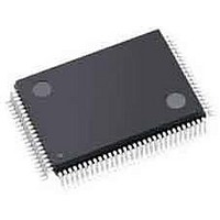
LFXP3C-3TN100C Lattice, LFXP3C-3TN100C Datasheet - Page 115

LFXP3C-3TN100C
Manufacturer Part Number
LFXP3C-3TN100C
Description
FPGA - Field Programmable Gate Array 3.1K LUTS 62 I/O
Manufacturer
Lattice
Datasheet
1.LFXP3C-3QN208C.pdf
(130 pages)
Specifications of LFXP3C-3TN100C
Number Of Programmable I/os
62
Data Ram Size
55296
Supply Voltage (max)
3.465 V
Maximum Operating Temperature
+ 90 C
Minimum Operating Temperature
0 C
Mounting Style
SMD/SMT
Supply Voltage (min)
1.71 V
Package / Case
TQFP-100
Lead Free Status / RoHS Status
Lead free / RoHS Compliant
Available stocks
Company
Part Number
Manufacturer
Quantity
Price
Company:
Part Number:
LFXP3C-3TN100C
Manufacturer:
E-SWITCH
Quantity:
14 000
Company:
Part Number:
LFXP3C-3TN100C
Manufacturer:
LATTICE
Quantity:
5 510
Company:
Part Number:
LFXP3C-3TN100C
Manufacturer:
Lattice Semiconductor Corporation
Quantity:
10 000
Pinout Information
Lattice Semiconductor
LatticeXP Family Data Sheet
Thermal Management
Thermal management is recommended as part of any sound FPGA design methodology. To assess the thermal
characteristics of a system, Lattice specifies a maximum allowable junction temperature in all device data sheets.
Designers must complete a thermal analysis of their specific design to ensure that the device and package do not
exceed the junction temperature limits. Refer to the Thermal Management document to find the device/package
specific thermal values.
For Further Information
For further information regarding Thermal Management, refer to the following located on the Lattice website at
www.latticesemi.com.
• Thermal Management document
• Technical Note TN1052 - Power Estimation and Management for LatticeECP/EC and LatticeXP Devices
• Power Calculator tool included with Lattice’s ispLEVER design tool, or as a standalone download from
www.latticesemi.com/software
4-56


