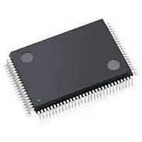
APA075-TQG100 Actel, APA075-TQG100 Datasheet - Page 75

APA075-TQG100
Manufacturer Part Number
APA075-TQG100
Description
FPGA - Field Programmable Gate Array 75K System Gates
Manufacturer
Actel
Datasheet
1.APA075-FGG144.pdf
(178 pages)
Specifications of APA075-TQG100
Processor Series
APA075
Core
IP Core
Maximum Operating Frequency
150 MHz
Number Of Programmable I/os
158
Data Ram Size
27648
Supply Voltage (max)
2.7 V
Maximum Operating Temperature
+ 70 C
Minimum Operating Temperature
0 C
Development Tools By Supplier
APA-Eval-Kit, APA-Eval-BRD1, Silicon-Explorer II, Silicon-Sculptor 3, SI-EX-TCA, Flashpro 4, Flashpro 3, Flashpro Lite
Mounting Style
SMD/SMT
Supply Voltage (min)
2.3 V
Number Of Gates
75 K
Package / Case
TQFP-100
Lead Free Status / RoHS Status
Lead free / RoHS Compliant
Available stocks
Company
Part Number
Manufacturer
Quantity
Price
Part Number:
APA075-TQG100
Manufacturer:
ACTEL
Quantity:
20 000
Company:
Part Number:
APA075-TQG100A
Manufacturer:
Microsemi SoC
Quantity:
10 000
Company:
Part Number:
APA075-TQG100I
Manufacturer:
Microsemi SoC
Quantity:
10 000
Part Number:
APA075-TQG100I
Manufacturer:
ACTEL/爱特
Quantity:
20 000
Asynchronous FIFO Full and Empty Transitions
The asynchronous FIFO accepts writes and reads while
not full or not empty. When the FIFO is full, all writes are
inhibited. Conversely, when the FIFO is empty, all reads
are inhibited. A problem is created if the FIFO is written
to during the transition from full to not full, or read
during the transition from empty to not empty. The
exact time at which the write or read operation changes
from inhibited to accepted after the read (write) signal
which causes the transition from full or empty to not full
or not empty is indeterminate. For slow cycles, this
indeterminate period starts 1 ns after the RB (WB)
transition, which deactivates full or not empty and ends
3 ns after the RB (WB) transition. For fast cycles, the
indeterminate period ends 3 ns (7.5 ns – RDL (WRL)) after
the RB (WB) transition, whichever is later
page
The timing diagram for write is shown in
page
Figure 2-36 on page
see
Table 2-62 • Memory Block FIFO Interface Signals
FIFO Signal
WCLKS
RCLKS
LEVEL [0:7]*
RBLKB
RDB
RESET
WBLKB
DI[0:8]
WRB
FULL, EMPTY
EQTH, GEQTH*
DO[0:8]
RPE
WPE
LGDEP [0:2]
PARODD
Note: *LEVEL is always eight bits (0000.0000, 0000.0001). That means for values of DEPTH greater than 256, not all values will be
Table 2-14 on page
2-4).
2-62. The timing diagram for read is shown in
possible, e.g. for DEPTH = 512, the LEVEL can only have the values 2, 4, . . ., 512. The LEVEL signal circuit will generate signals that
indicate whether the FIFO is exactly filled to the value of LEVEL (EQTH) or filled equal or higher (GEQTH) than the specified LEVEL.
Since counting starts at 0, EQTH will become true when the FIFO holds (LEVEL+1) words for 512-bit FIFOs.
2-63. For basic SRAM configurations,
Bits
2-22. When reset is asserted, the
1
1
8
1
1
1
1
9
1
2
2
9
1
1
3
1
In/Out
Out
Out
Out
Out
Out
In
In
In
In
In
In
In
In
In
In
In
Figure 2-35 on
(Table 2-1 on
Write clock used for synchronization on write side
Read clock used for synchronization on read side
Direct configuration implements static flag logic
Read block select (active Low)
Read pulse (active Low)
Reset for FIFO pointers (active Low)
Write block select (active Low)
Input data bits [0:8], [8] will be generated if PARGEN is true
Write pulse (active Low)
FIFO flags. FULL prevents write and EMPTY prevents read
EQTH is true when the FIFO holds the number of words specified by the LEVEL signal.
GEQTH is true when the FIFO holds (LEVEL) words or more
Output data bits [0:8]
Read parity error (active High)
Write parity error (active High)
Configures DEPTH of the FIFO to 2
Selects Odd parity generation/detect when high, Even when low
v5.9
empty flag will be asserted, the counters will reset, the
outputs go to zero, but the internal RAM is not erased.
Enclosed Timing Diagrams – FIFO Mode:
The following timing diagrams apply only to single cell;
they are not applicable to cascaded cells. For more
information, refer to the
application note.
•
•
•
•
•
•
"Asynchronous FIFO Read" section on page 2-67
"Asynchronous FIFO Write" section on page 2-68
"Synchronous FIFO Read, Access Timed Output
Strobe (Synchronous Transparent)" section on
page 2-69
"Synchronous FIFO Read, Pipeline Mode Outputs
(Synchronous Pipelined)" section on page 2-70
"Synchronous FIFO Write" section on page 2-71
"FIFO Reset" section on page 2-72
(LGDEP+1)
Description
ProASIC
ProASIC
PLUS
PLUS
Flash Family FPGAs
RAM/FIFO Blocks
2-65


