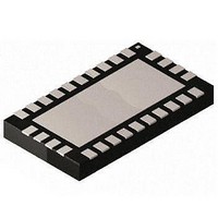
MAX2009ETI+ Maxim Integrated Products, MAX2009ETI+ Datasheet - Page 2

MAX2009ETI+
Manufacturer Part Number
MAX2009ETI+
Description
RF Wireless Misc IC RF PREDISTORT ADJ djustable RF Predist
Manufacturer
Maxim Integrated Products
Type
Adjustable RF Predistorterr
Datasheet
1.MAX2009ETI.pdf
(19 pages)
Specifications of MAX2009ETI+
Operating Frequency
1200 MHz to 2500 MHz
Supply Voltage (max)
5.25 V
Supply Voltage (min)
4.75 V
Supply Current
10 mA
Operating Temperature Range
- 40 C to + 85 C
Package / Case
TQFN-28
Mounting Style
SMD/SMT
Ic Function
Adjustable RF Predistorter
Supply Voltage Range
4.75V To 5.25V
Digital Ic Case Style
QFN
No. Of Pins
28
Filter Terminals
SMD
Rohs Compliant
Yes
Lead Free Status / RoHS Status
Lead free / RoHS Compliant
ABSOLUTE MAXIMUM RATINGS
V
ING, OUTG, GCS, GFS, GBP to GND......-0.3V to (V
INP, OUTP, PFS_, PDCS_, PBRAW,
Input (ING, INP, OUTP, OUTG) Level ............................+23dBm
PBEXP Output Current ........................................................±1mA
1200MHz to 2500MHz Adjustable
RF Predistorter
Stresses beyond those listed under “Absolute Maximum Ratings” may cause permanent damage to the device. These are stress ratings only, and functional
operation of the device at these or any other conditions beyond those indicated in the operational sections of the specifications is not implied. Exposure to
absolute maximum rating conditions for extended periods may affect device reliability.
DC ELECTRICAL CHARACTERISTICS
(MAX2009 EV kit; V
50Ω; V
+85°C. Typical values are at V
2
Supply Voltage
Supply Current
Analog Input Voltage Range
Analog Input Current
Logic-Input High Voltage
Logic-Input Low Voltage
Logic Input Current
CCG
PBEXP, PBIN to GND ............................-0.3V to (V
_______________________________________________________________________________________
, V
PF_S1
CCP
PARAMETER
to GND ..............................................-0.3V to +5.5V
= open; PBEXP shorted to PBRAW; V
CCG
= V
CCP
CCG
= +4.75V to +5.25V; no RF signal applied; INP, ING, OUTP, OUTG are AC-coupled and terminated to
= V
V
V
V
PBIN, PBRAW
GBP, GFS, GCS
V
V
V
PDCS1, PDCS2 (Note 1)
PDCS1, PDCS2 (Note 1)
CCP
CCG
CCP
CCG
GFS
GBP
PBIN
= +5.0V, T
, V
= V
= 0 to +5V
= 0 to +5V
CCP
GCS
PDCS1
= V
CCG
CCP
A
= +25°C, unless otherwise noted.)
PBRAW
+ 0.3V)
+ 0.3V)
= V
CONDITIONS
PDCS2
= 0V
= 0.8V; V
Continuous Power Dissipation (T
Operating Temperature Range ...........................-40°C to +85°C
Junction Temperature ......................................................+150°C
Storage Temperature Range .............................-65°C to +150°C
Lead Temperature (soldering 10s) ..................................+300°C
28-Pin Thin QFN-EP
(derate 21mW/°C above +70°C) ...............................1667mW
PBIN
= V
GBP
= V
GCS
= GND; V
-100
-100
MIN
4.75
2.0
-2
-2
0
0
A
= +70°C)
GFS
TYP
5.8
10
= V
CCG
V
V
+170
+220
MAX
5.25
12.1
CCG
0.8
CCP
+2
+2
7
; T
A
= -40°C to
UNITS
mA
µA
µA
V
V
V
V


