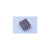
DG419BDQ-T1-E3 Vishay, DG419BDQ-T1-E3 Datasheet

DG419BDQ-T1-E3
Specifications of DG419BDQ-T1-E3
Related parts for DG419BDQ-T1-E3
DG419BDQ-T1-E3 Summary of contents
Page 1
... To achieve high-voltage ratings and superior switching performance, the DG417B series is built on Vishay Siliconix’s high voltage silicon gate (HVSG) process. Break- before-make is guaranteed for the DG419B, which is an SPDT configuration ...
Page 2
... DG418BDJ DG418BDJ-E3 DG417BDY DG417BDY-E3 DG417BDY-T1 DG417BDY-T1-E3 DG418BDY DG418BDY-E3 DG418BDY-T1 DG418BDY-T1-E3 DG417BDQ-T1-E3 DG418BDQ-T1-E3 DG419BDJ DG419BDJ-E3 DG419BDY DG419BDY-E3 DG419BDY-T1 DG419BDY-T1-E3 DG419BDQ-T1-E3 Limit - (GND - 0.3) to (V+) + 0 mA, whichever occurs first 30 100 - 65 to 150 400 400 400 600 Document Number: 72107 S09-1261-Rev. D, 13-Jul-09 Unit ...
Page 3
... 300 Ω DG419B Room ± Room = 0 Ω gen gen = 50 Ω pF Room MHz DG419B Room DG417B, DG418B, DG419B Vishay Siliconix Suffix D Suffix - 55 °C to 125 ° ° ° Typ. Min. Max. Min. Full - Full 34 - 0.25 0.25 - 0.25 - 0.1 Full - 0.25 0.25 - 0.25 - 0.1 ...
Page 4
... DG417B, DG418B, DG419B Vishay Siliconix a SPECIFICATIONS Parameter Symbol Dynamic Characteristics e C Source Off Capacitance S(off) e Drain Off Capacitance C D(off) e Channel On Capacitance C D(on) Power Supplies Positive Supply Current I+ Negative Supply Current I- Logic Supply Current I L Ground Current I GND a SPECIFICATIONS Parameter Symbol Analog Switch ...
Page 5
... Document Number: 72107 S09-1261-Rev. D, 13-Jul- °C, unless otherwise noted ± = ± and Temperature 100 100 µ I D(on) I S(off) 100 n 100 DG417B, DG418B, DG419B Vishay Siliconix ° ± ± ± ± ± Drain Voltage (V) D On-Resistance vs. V and Dual Supply Voltage 125 ° ...
Page 6
... DG417B, DG418B, DG419B Vishay Siliconix TYPICAL CHARACTERISTICS T 140 120 100 ± Temperature ( C) Switching Time vs. Temperature 140 120 TRANS- 100 80 t TRANS Temperature ( C) Transition Time vs. Temperature 3 2.5 2.0 1.5 1.0 0.5 0 Supply Voltage (V) Switching Threshold vs. Supply Voltage www.vishay.com °C, unless otherwise noted ...
Page 7
... DG419B 100 Logic Input V O Switch Input 300 35 pF Switch Output Note: L DS(on) Figure 2. Switching Time (DG417B/418B) DG417B, DG418B, DG419B Vishay Siliconix 200 180 DG417B 160 140 120 100 Analog Voltage (V) Charge Injection vs. Analog Voltage (Measured at source pin) 200 180 ...
Page 8
... DG417B, DG418B, DG419B Vishay Siliconix TEST CIRCUITS + GND - GND - (includes fixture and stray capacitance DS(on GND - 15 V www.vishay.com 8 Logic Input 300 35 pF Switch Output C (includes fixture and stray capacitance) L Figure 3. Break-Before-Make (DG419B) Logic Input 300 Switch Output Figure 4. Transition Time (DG419B) ...
Page 9
... Vishay Siliconix maintains worldwide manufacturing capability. Products may be manufactured at one of several qualified locations. Reliability data for Silicon Technology and Package Reliability represent a composite of all qualified locations. For related documents such as package/tape drawings, part marking, and reliability data, see www.vishay.com/ppg?72107. Document Number: 72107 S09-1261-Rev ...
Page 10
... Vishay product could result in personal injury or death. Customers using or selling Vishay products not expressly indicated for use in such applications their own risk and agree to fully indemnify and hold Vishay and its distributors harmless from and against any and all claims, liabilities, expenses and damages arising or resulting in connection with such use or sale, including attorneys fees, even if such claim alleges that Vishay or its distributor was negligent regarding the design or manufacture of the part ...


