DG445DJ-E3 Vishay, DG445DJ-E3 Datasheet
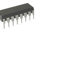
Analog Switch ICs SPST Analog Switch

DG445DJ-E3

Manufacturer Part Number
DG445DJ-E3
Description
Analog Switch ICs SPST Analog Switch
Manufacturer
Vishay
Type
Analog Switchr
Datasheets

Specifications of DG445DJ-E3

Number Of Switches
Quad
Switch Configuration
SPST
On Resistance (max)
160 Ohms
On Time (max)
450 ns
Off Time (max)
210 ns
Supply Voltage (max)
25 V
Supply Current
0.000001 mA
Maximum Power Dissipation
450 mW
Maximum Operating Temperature
+ 85 C
Mounting Style
Through Hole
Package / Case
PDIP-16
Minimum Operating Temperature
- 40 C
Analog Switch Type
SPST
No. Of Channels
4
On State Resistance Max
50ohm
Turn Off Time
160ns
Turn On Time
120ns
Supply Voltage Range
10.8V To 13.2V
Multiplexer Configuration
Quad SPST
Number Of Inputs
4
Number Of Outputs
4
Number Of Channels
4
Analog Switch On Resistance
160@10.8VOhm
Power Supply Requirement
Single/Dual
Single Supply Voltage (min)
13V
Single Supply Voltage (typ)
12/15/18/24/28V
Single Supply Voltage (max)
36V
Dual Supply Voltage (min)
±7V
Dual Supply Voltage (typ)
±9/±12/±15/±18V
Dual Supply Voltage (max)
±22V
Power Dissipation
450mW
Mounting
Through Hole
Pin Count
16
Operating Temp Range
-40C to 85C
Operating Temperature Classification
Industrial
Lead Free Status / RoHS Status
Lead free / RoHS Compliant
Lead Free Status / RoHS Status
Lead free / RoHS Compliant, Lead free / RoHS Compliant
The DG444/DG445 monolithic quad analog switches are
designed to provide high speed, low error switching of analog
signals. The DG444 has a normally closed function. The
DG445 has a normally open function. Combining low power
(22 nW, typ)
DG444/DG445 are ideally suited for upgrading DG211/212
sockets. Charge injection has been minimized on the drain for
use in sample-and-hold circuits.
Document Number: 70054
S-52433—Rev. F, 06-Sep-99
Low On-Resistance: 50
Low Leakage: 80 pA
Low Power Consumption: 22 nW
Fast Switching Action—t
Low Charge Injection
DG211/DG212 Upgrades
TTL/CMOS Logic Compatible
GND
IN
IN
D
V–
D
S
S
1
1
1
4
4
4
1
2
3
4
5
6
7
8
with
Dual-In-Line and SOIC
high speed (t
Top View
DG444
ON
Quad SPST CMOS Analog Switches
: 120 ns
ON
: 120 ns, typ), the
16
15
14
13
12
11
10
9
Low Signal Errors and Distortion
Reduced Power Supply
Requirements
Faster Throughput
Improved Reliability
Reduced Pedestal Errors
Simple Interfacing
IN
D
S
V+
V
S
D
IN
2
2
L
3
3
2
3
To achieve high-voltage ratings and superior switching
performance, the DG444/DG445 are built on Vishay Siliconix’s
high-voltage silicon-gate process. An epitaxial layer prevents
latchup.
Each switch conducts equally well in both directions when on,
and blocks input voltages to the supply levels when off.
Temp Range
–40 C to 85 C
–40 C to 85 C
40 C
85 C
Logic
0
1
Audio Switching
Battery Powered Systems
Data Acquisition
Sample-and-Hold Circuits
Telecommunication Systems
Automatic Test Equipment
Single Supply Circuits
Hard Disk Drives
16-Pin Narrow SOIC
16-Pin Narrow SOIC
16-Pin Plastic DIP
16-Pin Plastic DIP
Logic “0”
Logic “1”
Package
www.vishay.com FaxBack 408-970-5600
DG444
OFF
ON
Vishay Siliconix
0.8 V
2.4 V
DG444/445
DG445
Part Number
OFF
ON
DG444DJ
DG445DJ
DG444DY
DG445DY
4-1

Related parts for DG445DJ-E3

DG445DJ-E3 Summary of contents

Page 1

... Single Supply Circuits Hard Disk Drives Logic DG444 DG445 0 ON OFF 1 OFF ON Logic “0” 0.8 V Logic “1” 2.4 V Package Part Number DG444DJ 16-Pin Plastic DIP 16-Pin Plastic DIP DG445DJ DG444DY 16-Pin Narrow SOIC 16-Pin Narrow SOIC DG445DY www.vishay.com FaxBack 408-970-5600 4-1 ...

Page 2

... Channel On Capacitance C D(on) Power Supplies Positive Supply Current I+ Negative Supply Current I– Logic Supply Current I L Ground Current I GND www.vishay.com FaxBack 408-970-5600 4 Power Dissipation (Package)b c 16-Pin Plastic DIP 25 V 16-Pin Narrow Body SOIC (V–) – (V Notes: a. Signals diodes. Limit forward diode current to maximum current ratings. ...

Page 3

... Room Full Room Full Room Full Room Full DG444/445 Vishay Siliconix D Suffix – Min Typ Max Unit 100 160 200 300 450 200 2 pC 0.001 1 5 –1 –0.0001 – 0.001 1 5 –1 –0.001 –5 www.vishay.com FaxBack 408-970-5600 4-3 ...

Page 4

... Source/Drain Leakage Currents S(off) D(off) 0 –20 I D(on) –40 – V– = –15 V –80 For I (off) –100 –15 –10 – – Drain or Source Voltage ( www.vishay.com FaxBack 408-970-5600 4-4 Crosstak and Off Isolation vs. Frequency –140 –120 –100 –80 –60 –40 –20 0 100 V– –10 – ...

Page 5

... Switching Time vs. Input Voltage 160 V– = –15 V 140 t ON 120 100 OFF 60 DG444 40 DG445 Input Voltage (V) DG444/445 Vishay Siliconix V– DG444 DG445 OFF t OFF – Positive Supply ( V– = – S(on) D(on S(off) D(off) –10 – – Analog Voltage (V) ANALOG 5 www.vishay.com FaxBack 408-970-5600 4-5 ...

Page 6

... V– + V– GND – (includes fixture and stray capacitance + V– GND –15 V www.vishay.com FaxBack 408-970-5600 4-6 Level Shift/ Drive FIGURE Logic Input Switch Input 35 pF Switch 0 V Output Note: Logic input waveform is inverted for DG445. FIGURE 2. Switching Time OFF C (DG444 OFF ...

Page 7

... tantalum in parallel with 0.01 mF ceramic 0V GND V– C –15 V FIGURE 6. Source/Drain Capacitances + DG444 GND V– FIGURE 7. Level Shifter DG444/445 Vishay Siliconix + GND V– C – Off Isolation = 20 log V O FIGURE 5. Off Isolation Meter HP4192A Impedance Analyzer or Equivalent MHz + OUT www.vishay.com FaxBack 408-970-5600 4-7 ...

Page 8

... GAIN GAIN GAIN 100 V DG444 or DG445 V– –15 V FIGURE 8. Precision-Weighted Resistor Programmable-Gain Amplifier +15 V –15 V – 5 www.vishay.com FaxBack 408-970-5600 4-8 + – +15 V Gain error is determined only by the resistor tolerance. Op amp offset and CMRR will limit V+ L accuracy of circuit With OUT GND ...

Page 9

... Vishay disclaims any and all liability arising out of the use or application of any product described herein or of any information provided herein to the maximum extent permitted by law. The product specifications do not expand or otherwise modify Vishay’ ...

Related keywords