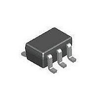
DG9411DL-T1-E3 Vishay, DG9411DL-T1-E3 Datasheet - Page 2

DG9411DL-T1-E3
Manufacturer Part Number
DG9411DL-T1-E3
Description
Analog Switch ICs SPDT Analog Switch
Manufacturer
Vishay
Datasheet
1.DG9411DL-T1-E3.pdf
(9 pages)
Specifications of DG9411DL-T1-E3
Number Of Switches
Single
Switch Configuration
SPDT
On Resistance (max)
35 Ohms
On Time (max)
40 ns
Off Time (max)
23 ns
Supply Voltage (max)
5.5 V
Supply Voltage (min)
4.5 V
Supply Current
0.00001 mA
Maximum Power Dissipation
250 mW
Maximum Operating Temperature
+ 85 C
Mounting Style
SMD/SMT
Package / Case
SC-70
Minimum Operating Temperature
- 40 C
Analog Switch Type
SPDT
No. Of Channels
1
On State Resistance Max
12ohm
Turn Off Time
5ns
Turn On Time
9ns
Supply Voltage Range
2.25V To 5.5V
Operating Temperature Range
-40°C To +85°C
Lead Free Status / RoHS Status
Lead free / RoHS Compliant
Lead Free Status / RoHS Status
Lead free / RoHS Compliant, Lead free / RoHS Compliant
Available stocks
Company
Part Number
Manufacturer
Quantity
Price
Company:
Part Number:
DG9411DL-T1-E3
Manufacturer:
VISHAY
Quantity:
673
Company:
Part Number:
DG9411DL-T1-E3
Manufacturer:
VISHAY
Quantity:
60 000
Company:
Part Number:
DG9411DL-T1-E3
Manufacturer:
Vishay
Quantity:
3 628
DG9411
Vishay Siliconix
Notes:
a. Signals on NC, NO, or COM or IN exceeding V+ will be clamped by internal diodes. Limit forward diode current to maximum current ratings.
b. All leads welded or soldered to PC Board.
c. Derate 3.1 mW/°C above 70 °C.
www.vishay.com
2
ABSOLUTE MAXIMUM RATINGS
Parameter
Reference V+ to GND
IN, COM, NC, NO
Continuous Current (Any Terminal)
Peak Current (Pulsed at 1 ms, 10 % duty cycle)
Storage Temperature
Power Dissipation (Packages)
SPECIFICATIONS V+ = 2.5 V
Parameter
Analog Switch
Analog Signal Range
Drain-Source On-Resistance
r
Switch Off
Leakage Current
Channel-On
Leakage Current
Digital Control
Input High Voltage
Input Low Voltage
Input Capacitance
Input Current
Dynamic Characteristics
Turn-On Time
Turn-Off Time
Break-Before-Make Time
Charge Injection
Off-Isolation
Crosstalk
Source-Off Capacitance
Channel-On Capacitance
Drain-to-Source Capacitance
Power Supply
Power Supply Range
Power Supply Current
Power Consumption
DS(on)
Flatness
d
d
d
d
f
f
a
d
d
d
d
d
d
b
I
V
INL
Flatness
Symbol
C
NO
r
r
C
X
C
V
OIRR
I
I
DS(on)
DS(on)
I
V
Q
V
t
DS(off)
S(off)
D(off)
D(on)
t
C
OFF
TALK
S(off)
D(on)
V+
P
COM
or I
ON
I+
INH
t
, V
INL
INJ
d
in
C
NC
INH
6-Pin SC70
V+ = 2.75 V, V
C
L
V
D
= 1 nF, V
V+ = 2.25 V, V
V+ = 2.75 V, V
or V
R
Unless Otherwise Specified
L
c
S
= 50 Ω, C
V
= 1.5 V, R
IN
GEN
V+ = 2.5 V, ± 10 %
V
S
Test Conditions
= 0 or V+, f = 1 MHz
Figures 1 and 2
IN
= 0.5 V/1.5 V, V
V
= 0 V, V
= 0.4 or 2.0 V
V+ = 2.5 V
IN
Figure 3
D
S
L
= 0 or V+
V
= 1.0 V, I
L
= 5 pF, f = 1 MHz
= V
IN
= 300 Ω, C
S
= 0 or V+
D
= 0 V, R
= 0.5 V/1.5 V
S
e
D
= 10 mA
= 1.5 V/0.5 V
L
GEN
= 35 pF
= 0 Ω,
- 0.3 to (V+ + 0.3)
- 0.3 to + 6
- 65 to 150
Temp
Room
Room
Room
Room
Room
Room
Room
Room
Room
Room
Room
Room
Room
Room
Full
Full
Full
Full
Full
Full
Full
Full
Full
Full
Full
± 200
Limit
± 50
250
d
d
d
d
d
a
d
- 250
- 250
- 250
Min
- 3.0
- 3.0
- 3.0
2.25
- 1
0
2
1
b
- 40 to 85 °C
S-72609-Rev. D, 24-Dec-07
Document Number: 71347
Limits
Typ
0.01
- 73
- 70
26
29
10
16
12
20
20
3
7
5
7
c
Max
2.75
250
250
250
3.0
3.0
3.0
0.4
1.0
0.3
V+
35
40
40
45
23
28
10
1
Unit
mW
b
mA
°C
V
Unit
µW
pA
nA
pA
nA
pA
nA
µA
pC
dB
µA
pF
ns
pF
Ω
V
V
V


