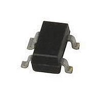
BFG520/XR,235 NXP Semiconductors, BFG520/XR,235 Datasheet - Page 7

BFG520/XR,235
Manufacturer Part Number
BFG520/XR,235
Description
TRANS RF NPN 9GHZ 15V SOT143
Manufacturer
NXP Semiconductors
Datasheet
1.BFG520XR235.pdf
(14 pages)
Specifications of BFG520/XR,235
Package / Case
SC-61AA, SOT143R
Transistor Type
NPN
Voltage - Collector Emitter Breakdown (max)
15V
Frequency - Transition
9GHz
Noise Figure (db Typ @ F)
1.1dB ~ 2.1dB @ 900MHz
Power - Max
300mW
Dc Current Gain (hfe) (min) @ Ic, Vce
60 @ 20mA, 6V
Current - Collector (ic) (max)
70mA
Mounting Type
Surface Mount
Dc Collector/base Gain Hfe Min
60
Dc Current Gain Hfe Max
250
Mounting Style
SMD/SMT
Configuration
Single
Transistor Polarity
NPN
Collector- Emitter Voltage Vceo Max
15 V
Emitter- Base Voltage Vebo
2.5 V
Continuous Collector Current
70 mA
Power Dissipation
300 mW
Lead Free Status / RoHS Status
Lead free / RoHS Compliant
Gain
-
Lead Free Status / RoHS Status
Lead free / RoHS Compliant, Lead free / RoHS Compliant
NXP Semiconductors
handbook, halfpage
handbook, halfpage
NPN 9 GHz wideband transistor
Fig.11 Intermodulation distortion as a function of
V
Fig.13 Minimum noise figure and associated
CE
F min
(dB)
(dB)
d im
= 6 V; T
20
30
40
50
60
70
5
4
3
2
1
0
0
1
2000 MHz
1000 MHz
collector current.
available gain as functions of collector
current.
900 MHz
500 MHz
amb
= 25 C.
10
F min
20
10
G ass
30
I C (mA)
f = 900 MHz
1000 MHz
2000 MHz
40
I C (mA)
MEA975
MRA682
Rev. 04 - 23 November 2007
50
10
20
15
10
0
G ass
5
2
(dB)
5
handbook, halfpage
handbook, halfpage
Fig.12 Second order intermodulation distortion as
V
Fig.14 Minimum noise figure and associated
CE
BFG520; BFG520/X; BFG520/XR
F min
(dB)
(dB)
d 2
= 6 V; T
20
30
40
50
60
70
5
4
3
2
1
0
10
0
20 mA
2
a function of collector current.
available gain as functions of frequency.
5 mA
amb
= 25 C.
I C = 5 mA
10
F min
20
20 mA
10
G ass
3
30
f (MHz)
Product specification
40
I C (mA)
MEA974
MRA683
7 of 14
50
10
20
15
10
0
5
4
G ass
(dB)
5


