MC56F8255VLD Freescale Semiconductor, MC56F8255VLD Datasheet - Page 34
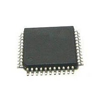
MC56F8255VLD
Manufacturer Part Number
MC56F8255VLD
Description
DSC 64K FLASH 60MHZ 44-LQFP
Manufacturer
Freescale Semiconductor
Series
56F8xxxr
Datasheets
1.TWR-56F8257.pdf
(88 pages)
2.MC56F8245VLD.pdf
(14 pages)
3.MC56F8245VLD.pdf
(2 pages)
4.MC56F8245VLD.pdf
(629 pages)
Specifications of MC56F8255VLD
Core Processor
56800E
Core Size
16-Bit
Speed
60MHz
Connectivity
CAN, I²C, LIN, SCI, SPI
Peripherals
LVD, POR, PWM, WDT
Number Of I /o
35
Program Memory Size
64KB (32K x 16)
Program Memory Type
FLASH
Ram Size
4K x 16
Voltage - Supply (vcc/vdd)
3 V ~ 3.6 V
Data Converters
A/D 8x12b, D/A 1x12b
Oscillator Type
Internal
Operating Temperature
-40°C ~ 105°C
Package / Case
44-LQFP
Product
DSCs
Processor Series
56800E
Core
56800E
Device Million Instructions Per Second
60 MIPs
Maximum Clock Frequency
60 MHz
Number Of Programmable I/os
35
Data Ram Size
8 KB
Operating Supply Voltage
3.3 V
Maximum Operating Temperature
+ 105 C
Mounting Style
SMD/SMT
Minimum Operating Temperature
- 40 C
On-chip Adc
12 bit, 4 Channel
Lead Free Status / RoHS Status
Lead free / RoHS Compliant
Eeprom Size
-
Lead Free Status / Rohs Status
Details
Available stocks
Company
Part Number
Manufacturer
Quantity
Price

Company:
Part Number:
MC56F8255VLD
Manufacturer:
Freescale Semiconductor
Quantity:
10 000


Memory Maps
By default, the chip reset address and COP reset address correspond to vector 0 and 1 of the interrupt vector table. In these
instances, the first two locations in the vector table must contain branch or JMP instructions. All other entries must contain JSR
instructions.
Table 48 on page 85
4.5
The locations of on-chip peripheral registers are part of the data memory map on the 56800E series. These locations may be
accessed with the same addressing modes used for ordinary data memory. However, all peripheral registers should be read or
written using word accesses only.
Table 12
listed in order of the base address.
34
•
The 56F824x’s startup address is located at 0x00 2000. The reset value of VBA is reset to a value of 0x0020 that
corresponds to the address 0x00 2000.
summarizes the base addresses for the set of peripherals on the MC56F825x/MC56F824x devices. Peripherals are
Peripheral Memory-Mapped Registers
Quad Timer A
Quad Timer B
Analog-to-Digital Converter
Interrupt Controller
System Integration Module
Crossbar module
Computer Operating Properly module
On-Chip Clock Synthesis module
Power Supervisor
GPIO Port A
GPIO Port B
GPIO Port C
GPIO Port D
GPIO Port E
GPIO Port F
12-bit Digital-to-Analog Converter
Analog Comparator A
Analog Comparator B
Analog Comparator C
Queued Serial Communication Interface 0
Queued Serial Communication Interface 1
Queued Serial Peripheral Interface
Inter-Integrated Circuit 0
Inter-Integrated Circuit 1
provides the MC56F825x/MC56F824x’s interrupt table contents and interrupt priority structure.
Table 12. Data Memory Peripheral Base Address Map Summary
Peripheral
MC56F825x/MC56F824x Digital Signal Controller, Rev. 3
GPIOB
GPIOC
GPIOD
GPIOE
GPIOA
GPIOF
CMPC
QSCI0
QSCI1
Prefix
TMRA
TMRB
OCCS
CMPB
XBAR
CMPA
QSPI
INTC
ADC
COP
DAC
I
I
SIM
2
2
PS
C0
C1
Base Address
X:0x00 F0C0
X:0x00 F0E0
X:0x00 F1A0
X:0x00 F1B0
X:0x00 F1C0
X:0x00 F1D0
X:0x00 F1E0
X:0x00 F000
X:0x00 F040
X:0x00 F080
X:0x00 F100
X:0x00 F110
X:0x00 F120
X:0x00 F130
X:0x00 F140
X:0x00 F150
X:0x00 F160
X:0x00 F170
X:0x00 F180
X:0x00 F190
X:0x00 F1F0
X:0x00 F200
X:0x00 F210
X:0x00 F220
Freescale Semiconductor
Related parts for MC56F8255VLD
Image
Part Number
Description
Manufacturer
Datasheet
Request
R

Part Number:
Description:
Manufacturer:
Freescale Semiconductor, Inc
Datasheet:
Part Number:
Description:
Manufacturer:
Freescale Semiconductor, Inc
Datasheet:
Part Number:
Description:
Manufacturer:
Freescale Semiconductor, Inc
Datasheet:
Part Number:
Description:
Manufacturer:
Freescale Semiconductor, Inc
Datasheet:
Part Number:
Description:
Manufacturer:
Freescale Semiconductor, Inc
Datasheet:
Part Number:
Description:
Manufacturer:
Freescale Semiconductor, Inc
Datasheet:
Part Number:
Description:
Manufacturer:
Freescale Semiconductor, Inc
Datasheet:
Part Number:
Description:
Manufacturer:
Freescale Semiconductor, Inc
Datasheet:
Part Number:
Description:
Manufacturer:
Freescale Semiconductor, Inc
Datasheet:
Part Number:
Description:
Manufacturer:
Freescale Semiconductor, Inc
Datasheet:
Part Number:
Description:
Manufacturer:
Freescale Semiconductor, Inc
Datasheet:
Part Number:
Description:
Manufacturer:
Freescale Semiconductor, Inc
Datasheet:
Part Number:
Description:
Manufacturer:
Freescale Semiconductor, Inc
Datasheet:
Part Number:
Description:
Manufacturer:
Freescale Semiconductor, Inc
Datasheet:
Part Number:
Description:
Manufacturer:
Freescale Semiconductor, Inc
Datasheet: