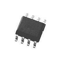
LM7171AIM National Semiconductor, LM7171AIM Datasheet - Page 16

LM7171AIM
Manufacturer Part Number
LM7171AIM
Description
IC, OP-AMP, 200MHZ, 4100V/µs, SOIC-8
Manufacturer
National Semiconductor
Datasheet
1.LM7171BINNOPB.pdf
(20 pages)
Specifications of LM7171AIM
Op Amp Type
Voltage Feedback
No. Of Amplifiers
1
Bandwidth
200MHz
Slew Rate
4100V/µs
Supply Voltage Range
5.5V To 36V
Amplifier Case Style
SOIC
No. Of Pins
8
Lead Free Status / RoHS Status
Contains lead / RoHS non-compliant
Available stocks
Company
Part Number
Manufacturer
Quantity
Price
Part Number:
LM7171AIM
Manufacturer:
NS/国半
Quantity:
20 000
Part Number:
LM7171AIMX
Manufacturer:
TI/德州仪器
Quantity:
20 000
Part Number:
LM7171AIMX/NOPB
Manufacturer:
TI/德州仪器
Quantity:
20 000
www.national.com
Application Notes
PERFORMANCE DISCUSSION
The LM7171 is a very high speed, voltage feedback ampli-
fier. It consumes only 6.5 mA supply current while providing
a unity-gain bandwidth of 200 MHz and a slew rate of
4100V/µs. It also has other great features such as low
differential gain and phase and high output current.
The LM7171 is a true voltage feedback amplifier. Unlike
current feedback amplifiers (CFAs) with a low inverting input
impedance and a high non-inverting input impedance, both
inputs of voltage feedback amplifiers (VFAs) have high im-
pedance nodes. The low impedance inverting input in CFAs
and a feedback capacitor create an additional pole that will
lead to instability. As a result, CFAs cannot be used in
traditional op amp circuits such as photodiode amplifiers,
I-to-V converters and integrators where a feedback capacitor
is required.
CIRCUIT OPERATION
The class AB input stage in LM7171 is fully symmetrical and
has a similar slewing characteristic to the current feedback
amplifiers. In the LM7171 Simplified Schematic, Q1 through
Q4 form the equivalent of the current feedback input buffer,
R
buffers the inverting input. The triple-buffered output stage
isolates the gain stage from the load to provide low output
impedance.
SLEW RATE CHARACTERISTIC
The slew rate of LM7171 is determined by the current avail-
able to charge and discharge an internal high impedance
node capacitor. This current is the differential input voltage
divided by the total degeneration resistor R
slew rate is proportional to the input voltage level, and the
higher slew rates are achievable in the lower gain configu-
rations. A curve of slew rate versus input voltage level is
provided in the “Typical Performance Characteristics”.
When a very fast large signal pulse is applied to the input of
an amplifier, some overshoot or undershoot occurs. By plac-
ing an external resistor such as 1 kΩ in series with the input
of LM7171, the bandwidth is reduced to help lower the
overshoot.
SLEW RATE LIMITATION
If the amplifier’s input signal has too large of an amplitude at
too high of a frequency, the amplifier is said to be slew rate
limited; this can cause ringing in time domain and peaking in
frequency domain at the output of the amplifier.
In the “Typical Performance Characteristics” section, there
are several curves of A
signal levels. For the A
and the LM7171 responds identically to the different input
signal levels of 30 mV, 100 mV and 300 mV.
For the A
peaking at high frequency (
input signal at high enough frequency that exceeds the
amplifier’s slew rate. The peaking in frequency response
does not limit the pulse response in time domain, and the
LM7171 is stable with noise gain of ≥+2.
E
the equivalent of the feedback resistor, and stage A
V
= +2 curves, with slight peaking occurs. This
V
V
= +4 curves, no peaking is present
= +2 and A
>
100 MHz) is caused by a large
V
= +4 versus input
E
. Therefore, the
16
LAYOUT CONSIDERATION
Printed Circuit Board and High Speed Op Amps
There are many things to consider when designing PC
boards for high speed op amps. Without proper caution, it is
very easy to have excessive ringing, oscillation and other
degraded AC performance in high speed circuits. As a rule,
the signal traces should be short and wide to provide low
inductance and low impedance paths. Any unused board
space needs to be grounded to reduce stray signal pickup.
Critical components should also be grounded at a common
point to eliminate voltage drop. Sockets add capacitance to
the board and can affect high frequency performance. It is
better to solder the amplifier directly into the PC board
without using any socket.
Using Probes
Active (FET) probes are ideal for taking high frequency
measurements because they have wide bandwidth, high
input impedance and low input capacitance. However, the
probe ground leads provide a long ground loop that will
produce errors in measurement. Instead, the probes can be
grounded directly by removing the ground leads and probe
jackets and using scope probe jacks.
Component Selection and Feedback Resistor
It is important in high speed applications to keep all compo-
nent leads short. For discrete components, choose carbon
composition-type resistors and mica-type capacitors. Sur-
face mount components are preferred over discrete compo-
nents for minimum inductive effect.
Large values of feedback resistors can couple with parasitic
capacitance and cause undesirable effects such as ringing
or oscillation in high speed amplifiers. For LM7171, a feed-
back resistor of 510Ω gives optimal performance.
COMPENSATION FOR INPUT CAPACITANCE
The combination of an amplifier’s input capacitance with the
gain setting resistors adds a pole that can cause peaking or
oscillation. To solve this problem, a feedback capacitor with
a value
can be used to cancel that pole. For LM7171, a feedback
capacitor of 2 pF is recommended. Figure 1 illustrates the
compensation circuit.
POWER SUPPLY BYPASSING
Bypassing the power supply is necessary to maintain low
power supply impedance across frequency. Both positive
and negative power supplies should be bypassed individu-
FIGURE 1. Compensating for Input Capacitance
C
F
>
(R
G
x C
IN
)/R
F
01238510


