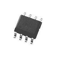
LM4865M National Semiconductor, LM4865M Datasheet - Page 11

LM4865M
Manufacturer Part Number
LM4865M
Description
IC, AUDIO PWR AMP, CLASS AB 750mW, SOIC8
Manufacturer
National Semiconductor
Datasheet
1.LM4865M.pdf
(16 pages)
Specifications of LM4865M
Audio Control Type
Volume
Output Power
1W
Control / Process Application
GSM Phones And Accessories, DECT, Office Phones, Hand Held Radio
Supply Voltage Range
2.7V To 5.5V
No. Of Channels
1
Thd + N
0.6% @ 8ohm, VDD=5V
Load Impedance
8ohm
Operating Temperature Range
-40°C To +85°C
Amplifier Case Style
MSOP
Rohs Compliant
Yes
Lead Free Status / RoHS Status
Contains lead / RoHS non-compliant
Available stocks
Company
Part Number
Manufacturer
Quantity
Price
Part Number:
LM4865M
Manufacturer:
NS/国半
Quantity:
20 000
Part Number:
LM4865M/NOPB
Manufacturer:
TI/德州仪器
Quantity:
20 000
Company:
Part Number:
LM4865MM
Manufacturer:
NSC
Quantity:
19 000
Company:
Part Number:
LM4865MM
Manufacturer:
NSC
Quantity:
9 500
Company:
Part Number:
LM4865MM
Manufacturer:
NS
Quantity:
9 500
Part Number:
LM4865MM
Manufacturer:
NS/国半
Quantity:
20 000
Part Number:
LM4865MMX
Manufacturer:
NS/国半
Quantity:
20 000
Part Number:
LM4865MX
Manufacturer:
NS/国半
Quantity:
20 000
Application Information
an external 1kΩ - 5kΩ resistor can be placed in parallel with
the internal 20kΩ resistor. The tradeoff for using this resistor
is increased quiescent current.
RECOMMENDED PRINTED CIRCUIT BOARD LAYOUT
Figure 4 through Figure 6 show the recommended two-layer
PC board layout that is optimized for the SO-8 packaged
LM4865 and associated external components. Figure 7
through Figure 11 show the recommended four-layer PC
board layout for the micro SMD packaged LM4865. A
four-layer board is recommended when using the micro
SMD packaged LM4865: the two inner layers, one con-
nected to the GND pin, the other to the V
heatsinking. Both layouts are designed for use with an ex-
ternal 5V supply, 8Ω speakers, and 32Ω headphones. The
schematic for both recommended PC board layouts is Figure
1.
Both circuit boards are easy to use. Apply a 5V supply
voltage and ground to the board’s V
respectively. Connect a speaker with an 8Ω minimum imped-
ance between the board’s -OUT and +OUT pads. For head-
phone use, the layout has provisions for a headphone jack,
J1. When a jack is connected as shown, inserting a head-
phone plug automatically switches off the external speaker.
FIGURE 4. Recommended SO PC board layout:
component side silkscreen
DD
(Continued)
and GND pads,
DD
pin, provide
10102538
11
FIGURE 5. Recommended SO PC board layout:
FIGURE 6. Recommended SO PC board layout:
component side layout
bottom side layout
www.national.com
10102539
10102540


