LMH2180YD National Semiconductor, LMH2180YD Datasheet
LMH2180YD
Specifications of LMH2180YD
Available stocks


Related parts for LMH2180YD

LMH2180YD Summary of contents
Page 1
... The LMH2180 is produced in the tiny 8-pin LLP solder bump and no pullback packages minimizing the required PCB space. National’s advanced packaging offers direct PCB-IC evaluation via pin access. Typical Application © 2008 National Semiconductor Corporation Features (Typical values are: V otherwise specified.) ■ ...
Page 2
... Absolute Maximum Ratings If Military/Aerospace specified devices are required, please contact the National Semiconductor Sales Office/ Distributors for availability and specifications. Supply Voltages (V + – V − ) ESD Tolerance Human Body (Note 4) Machine Model (Note 5) Charged Device Model Storage Temperature Range 2.7V Electrical Characteristics ...
Page 3
Symbol Parameter Miscellaneous Performance R Input Resistance per Buffer IN C Input Capacitance per Buffer IN Z Input Impedance IN V Output Swing Positive O Output Swing Negative I Output Short-Circuit Current SC (Notes 10, 11) V Enable High Active ...
Page 4
Symbol Parameter PSRR Power Supply Rejection Ratio A Small Signal Voltage Gain CL V Output Offset Voltage Temperature Coefficient Output OS Offset Voltage (Note 9) R Output Resistance OUT Miscellaneous Performance R Input Resistance per Buffer IN ...
Page 5
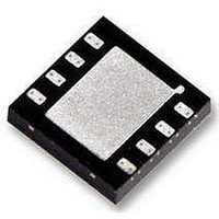
... Enable buffer 2 Ground connection SS Output 2 Output 1 Enable buffer 1 8-Pin LLP Top View Package Marking 1k Units Tape and Reel LMH2180YD 4.5k Units Tape and Reel 1k Units Tape and Reel LMH2180SD 4.5 Units Tape and Reel 5 30024601 Description 30024631 Transport Media NSC Drawing ...
Page 6
Typical Performance Characteristics R = 30kΩ and C = 10nF, unless otherwise specified. L COUPLING Frequency Response Frequency Response Over Temperature Phase Response Over Temperature www.national.com T = 25° 2.7V Phase Response 30024603 Frequency ...
Page 7
Large Signal Bandwidth Voltage Noise Isolation Output to Input vs. Frequency Gain Flatness < 0.1 dB (GFN) 30024609 Phase Noise 30024611 Crosstalk Rejection vs. Frequency 30024613 7 30024610 30024612 30024614 www.national.com ...
Page 8
Transient Response Positive Small Signal Pulse Response Large Signal Response www.national.com Transient Response Negative 30024615 Small Signal Pulse Response 30024617 Large Signal Response 30024619 8 30024616 30024618 30024620 ...
Page 9
I vs. V SUPPLY SUPPLY 30024621 I vs. V SUPPLY SUPPLY 30024623 V vs SUPPLY 30024625 I vs. V SUPPLY SUPPLY PSRR vs. Frequency R vs. Frequency OUT 9 30024622 30024624 30024626 www.national.com ...
Page 10
Input Impedance vs. Frequency V vs. I (Sourcing) OUT OUT V vs. I (Sinking) OUT OUT www.national.com V OUT 30024627 V OUT 30024629 I Sourcing vs 30024632 10 vs. I (Sourcing) OUT 30024628 vs. I (Sinking) OUT 30024630 ...
Page 11
I Sinking vs. V Over Temperature SC SUPPLY I vs. V SUPPLY ENABLE I SUPPLY 30024634 30024636 11 vs. V ENABLE 30024635 www.national.com ...
Page 12
Application Information GENERAL The LMH2180 is designed to minimize the effects of spurious signals from the base chip to the oscillator. Also the influence of varying load resistance and capacitance to the oscillator is minimized, while the drive capability is ...
Page 13
PHASE NOISE A clock buffer adds noise to the clock signal. This noise caus- es uncertainty in the phase of the clock signal. This uncer- tainty is described by jitter (time domain) or phase noise (frequency domain). Communication systems, such ...
Page 14
Physical Dimensions www.national.com inches (millimeters) unless otherwise noted 8-Pin LLP NS Package Number YDA08A 8–Pin LLP NS Package Number SDA08A 14 ...
Page 15
Notes 15 www.national.com ...
Page 16
... For more National Semiconductor product information and proven design tools, visit the following Web sites at: Products Amplifiers www.national.com/amplifiers Audio www.national.com/audio Clock Conditioners www.national.com/timing Data Converters www.national.com/adc Displays www.national.com/displays Ethernet www.national.com/ethernet Interface www.national.com/interface LVDS www.national.com/lvds Power Management www.national.com/power Switching Regulators www.national.com/switchers LDOs www ...