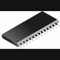
DS14C535MSA National Semiconductor, DS14C535MSA Datasheet - Page 5

DS14C535MSA
Manufacturer Part Number
DS14C535MSA
Description
IC, RS-232 TRANSCEIVER, 5.5V, SSOP-28
Manufacturer
National Semiconductor
Datasheet
1.DS14C535MSA.pdf
(8 pages)
Specifications of DS14C535MSA
Device Type
Driver / Receiver
Ic Interface Type
RS232
No. Of Drivers
3
Supply Voltage Range
4.5V To 5.5V
Driver Case Style
SSOP
No. Of Pins
28
Operating Temperature Range
0°C To +70°C
Lead Free Status / RoHS Status
Contains lead / RoHS non-compliant
Available stocks
Company
Part Number
Manufacturer
Quantity
Price
Part Number:
DS14C535MSA
Manufacturer:
NS/国半
Quantity:
20 000
Company:
Part Number:
DS14C535MSAX
Manufacturer:
NS
Quantity:
10 000
Part Number:
DS14C535MSAX
Manufacturer:
NS/国半
Quantity:
20 000
Part Number:
DS14C535MSAX/NOPB
Manufacturer:
MAXIM/美信
Quantity:
20 000
Parameter Measurement Information
Pin Descriptions
V
V+ (Pin 1). Positive supply for EIA/TIA-232-E drivers. Rec-
ommended external capacitor — 0.1 µF (16V). This supply is
not intended to be loaded externally.
V− (Pin 25). Negative supply for EIA/TIA-232-E drivers.
Recommended external capacitor — 0.1 µF (16V). This sup-
ply is not intended to be loaded externally.
C1+, C1− (Pins 2, 4). External capacitor connection pins.
C2+, C2− (Pins 28, 26). External capacitor connection pins.
SHUTDOWN (SD) (Pin 23). A High on the SHUTDOWN pin
will lower the total I
low power state. In this mode receiver R5 remains active.
The SD pin should be driven or tied low (GND) to disable the
shutdown mode.
D
D
EIA/TlA-232 -E levels.
CC
IN
OUT
1–3 (Pins 7, 8, 9). Driver input pins.
(Pin 3). Power supply pin for the device, +5V (
1–3 (Pins 22, 21, 20). Driver output pins conform to
CC
current to less than 10 µA, providing a
FIGURE 7. Receiver SHUTDOWN (SD) Delay Test Circuit
FIGURE 8. Receiver SHUTDOWN (SD) Delay Timing
FIGURE 6. Driver SHUTDOWN (SD) Delay Timing
±
0.5V).
5
(Continued)
R
EIA/TIA-232-E input voltages (
hysteresis of TBD mV. Unused receiver input pins may be
left open. Internal input resistor (5 kΩ) pulls input LOW,
providing a failsafe HIGH output.
R
GND (Pins 5, 27). Ground Pins. Both pins must be con-
nected to external ground. These pins are not connected
together on the chip.
Application Information
In a typical Data Terminal Equipment (DTE) to Data Circuit-
Terminating Equipment (DCE) 9-pin de-facto interface imple-
mentation, 2 data lines and 6 control lines are required. The
data lines are TXD and RXD and the control lines are RTS,
DTR, DSR, DCD, CTS and RI. The DS14C535 is a 3 x 5
Driver/Receiver and offers a single chip solution for the DTE
interface as shown in Figure 9.
Ring Indicator (RI) is used to inform the DTE that an incom-
ing call is coming from a remote DCE. When the DS14C535
IN
OUT
1–5 (Pins 19, 18, 17, 16, 15). Receiver input pins accept
1–5 (Pins 10, 11, 12, 13, 14). Receiver output pins.
01191010
01191009
01191008
±
25V). Receivers guarantees
www.national.com


