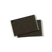
S29JL032H90TFI320 Spansion Inc., S29JL032H90TFI320 Datasheet - Page 13

S29JL032H90TFI320
Manufacturer Part Number
S29JL032H90TFI320
Description
IC, FLASH, 32MBIT, 90NS, TSOP-48
Manufacturer
Spansion Inc.
Datasheet
1.S29JL032H90TFI320.pdf
(61 pages)
Specifications of S29JL032H90TFI320
Memory Type
Flash
Memory Size
32Mbit
Memory Configuration
4M X 8 / 2M X 16
Ic Interface Type
CFI, Parallel
Access Time
90ns
Supply Voltage Range
2.7 To 3.6 V
Memory Case Style
TSOP
Data Bus Width
8 bit, 16 bit
Architecture
Boot Sector
Interface Type
Conventional
Supply Voltage (max)
3.6 V
Supply Voltage (min)
2.7 V
Maximum Operating Current
2 mA
Mounting Style
SMD/SMT
Operating Temperature
+ 85 C
Package / Case
TSOP-48
Rohs Compliant
YES
No. Of Pins
48
Lead Free Status / RoHS Status
Lead free / RoHS Compliant
Lead Free Status / RoHS Status
Lead free / RoHS Compliant, Lead free / RoHS Compliant
Available stocks
Company
Part Number
Manufacturer
Quantity
Price
Company:
Part Number:
S29JL032H90TFI320
Manufacturer:
Spansion
Quantity:
135
Company:
Part Number:
S29JL032H90TFI320
Manufacturer:
PANASONIC
Quantity:
4 314
Part Number:
S29JL032H90TFI320
Manufacturer:
SPANSION
Quantity:
20 000
8.
8.1
August 31, 2009 S29JL032H_00_B8
Device Bus Operations
Word/Byte Configuration
This section describes the requirements and use of the device bus operations, which are initiated through the
internal command register. The command register itself does not occupy any addressable memory location.
The register is a latch used to store the commands, along with the address and data information needed to
execute the command. The contents of the register serve as inputs to the internal state machine. The state
machine outputs dictate the function of the device.
control levels they require, and the resulting output. The following subsections describe each of these
operations in further detail.
Legend
L = Logic Low = V
H = Logic High = V
V
V
X = Don’t Care
SA = Sector Address
A
D
D
Notes
1. Addresses are A20:A0 in word mode (BYTE# = V
2. The sector protect and sector unprotect functions may also be implemented via programming equipment. See
3. If WP#/ACC = V
The BYTE# pin controls whether the device data I/O pins operate in the byte or word configuration. If the
BYTE# pin is set at logic ‘1’, the device is in word configuration, DQ15–DQ0 are active and controlled by CE#
and OE#.
If the BYTE# pin is set at logic ‘0’, the device is in byte configuration, and only data I/O pins DQ7–DQ0 are
active and controlled by CE# and OE#. The data I/O pins DQ14–DQ8 are tri-stated, and the DQ15 pin is used
as an input for the LSB (A-1) address function.
Read
Write
Standby
Output Disable
Reset
Sector Protect
(Note 2)
Sector Unprotect
(Note 2)
Temporary Sector
Unprotect
ID
HH
IN
IN
OUT
Protection and Unprotection on page
depends on whether they were last protected or unprotected using the method described in
Unprotection on page
= 8.5–12.5 V
= Address In
= Data In
= 9.0 ± 0.5 V
Operation
= Data Out
IL
IH
IL
, the two outermost boot sectors remain protected. If WP#/ACC = V
V
0.3 V
CE#
CC
X
X
L
L
L
L
L
22. If WP#/ACC = V
±
D a t a
OE#
H
X
H
X
H
H
X
L
Table 8.1 S29JL032H Device Bus Operations
WE# RESET# WP#/ACC
22.
H
X
H
X
X
L
L
L
S h e e t
HH
, all sectors will be unprotected.
V
0.3 V
V
V
V
CC
H
H
H
L
S29JL032H
ID
ID
ID
IH
±
), A20:A-1 in byte mode (BYTE# = V
(Note 3)
(Note 3)
(Note 3)
L/H
L/H
L/H
L/H
L/H
Table 8.1
A1 = H, A0 = L
A1 = H, A0 = L
SA, A6 = H,
Addresses
SA, A6 = L,
(Note 1)
A
A
A
X
X
X
lists the device bus operations, the inputs and
IN
IN
IN
BYTE# = V
IH
, protection on the two outermost boot sectors
IL
High-Z
High-Z
High-Z
D
).
D
D
OUT
X
X
IN
IN
Sector/Sector Block Protection and
IH
DQ15–DQ8
DQ14–DQ8 = High-Z,
BYTE# = V
DQ15 = A-1
High-Z
High-Z
High-Z
High-Z
Sector/Sector Block
X
X
IL
DQ7–DQ0
High-Z
High-Z
High-Z
D
D
D
D
D
OUT
IN
IN
IN
IN
13


