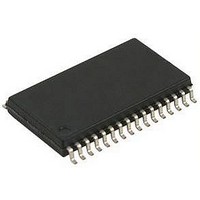
IS61LV25616AL-10TL INTEGRATED SILICON SOLUTION (ISSI), IS61LV25616AL-10TL Datasheet - Page 8

IS61LV25616AL-10TL
Manufacturer Part Number
IS61LV25616AL-10TL
Description
IC, SRAM, 4MBIT, 10NS, TSOP-2-44
Manufacturer
INTEGRATED SILICON SOLUTION (ISSI)
Datasheet
1.IS61LV25616AL-10BLI.pdf
(17 pages)
Specifications of IS61LV25616AL-10TL
Memory Size
4Mbit
Memory Configuration
256K X 16
Access Time
10ns
Supply Voltage Range
3.135V To 3.6V
Memory Case Style
TSOP-2
No. Of Pins
44
Operating Temperature Range
-40°C To +85°C
Lead Free Status / RoHS Status
Lead free / RoHS Compliant
Available stocks
Company
Part Number
Manufacturer
Quantity
Price
Company:
Part Number:
IS61LV25616AL-10TL
Manufacturer:
ISSI
Quantity:
1 000
Company:
Part Number:
IS61LV25616AL-10TL
Manufacturer:
ISSI
Quantity:
405
Part Number:
IS61LV25616AL-10TL
Manufacturer:
ISSI
Quantity:
20 000
Company:
Part Number:
IS61LV25616AL-10TLI
Manufacturer:
ISSI
Quantity:
2 000
Company:
Part Number:
IS61LV25616AL-10TLI
Manufacturer:
ISSI
Quantity:
8
Part Number:
IS61LV25616AL-10TLI
Manufacturer:
ISSI
Quantity:
20 000
WRITE CYCLE SWITCHING CHARACTERISTICS
Notes:
1. Test conditions assume signal transition times of 3 ns or less, timing reference levels of 1.5V, input pulse levels of
2. Tested with the load in Figure 2. Transition is measured ±500 mV from steady-state voltage. Not 100% tested.
3. The internal write time is defined by the overlap of CE LOW and UB or LB and WE LOW. All signals must be in
8
Notes:
1. WE is HIGH for a Read Cycle.
2. The device is continuously selected. OE, CE, UB, or LB = V
3. Address is valid prior to or coincident with CE LOW transition.
IS61LV25616AL
READ CYCLE NO. 2
Symbol
0V to 3.0V and output loading specified in Figure 1.
valid states to initiate a Write, but any one can go inactive to terminate the Write. The Data Input Setup and Hold
timing are referenced to the rising or falling edge of the signal that terminates the write.
t
t
t
t
t
t
t
t
t
t
t
t
WC
SCE
AW
HA
SA
PWB
PWE
PWE
SD
HD
HZWE
LZWE
1
2
(2)
(2)
ADDRESS
Parameter
Write Cycle Time
CE to Write End
Address Setup Time to Write End
Address Hold from Write End
Address Setup Time
LB, UB Valid to End of Write
WE Pulse Width
WE Pulse Width (OE = LOW)
Data Setup to Write End
Data Hold from Write End
WE LOW to High-Z Output
WE HIGH to Low-Z Output
LB, UB
Current
Supply
D
V
OUT
OE
CE
DD
(1,3)
HIGH-Z
t
LZCE
t
LZB
t
PU
t
AA
50%
t
DOE
t
t
LZOE
t
ACE
Integrated Silicon Solution, Inc. — www.issi.com —
BA
t
IL
RC
.
Min. Max.
10
10
—
8
8
0
0
8
8
6
0
2
-10
(1,3)
t
RC
—
—
—
—
—
—
—
—
—
—
—
DATA VALID
(Over Operating Range)
5
Min. Max.
12
12
—
8
8
0
0
8
8
6
0
2
-12
t
HZCE
—
—
—
—
—
—
—
—
—
—
—
6
t
PD
t
t
t
OHA
HZB
HZOE
50%
Unit
ns
ns
ns
ns
ns
ns
ns
ns
ns
ns
ns
ns
UB_CEDR2.eps
I
I
CC
SB
ISSI
1-800-379-4774
02/14/06
Rev. E
®


