PIC16F1827-I/MV Microchip Technology, PIC16F1827-I/MV Datasheet - Page 143
PIC16F1827-I/MV
Manufacturer Part Number
PIC16F1827-I/MV
Description
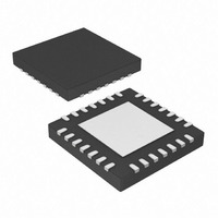
IC, 8BIT MCU, PIC16F, 32MHZ, QFN-28
Manufacturer
Microchip Technology
Series
PIC® XLP™ 16Fr
Datasheets
1.PIC16F722-ISS.pdf
(8 pages)
2.PIC16F1826-IP.pdf
(406 pages)
3.PIC16F1826-IP.pdf
(12 pages)
4.PIC16F1826-IP.pdf
(8 pages)
5.PIC16F1826-IP.pdf
(40 pages)
6.PIC16LF1827-ISS.pdf
(400 pages)
Specifications of PIC16F1827-I/MV
Controller Family/series
PIC16F
Eeprom Memory Size
256Byte
Ram Memory Size
384Byte
Cpu Speed
32MHz
No. Of Timers
5
Interface
EUSART, I2C, SPI
Core Size
8 Bit
Program Memory Size
4kWords
Core Processor
PIC
Speed
32MHz
Connectivity
I²C, SPI, UART/USART
Peripherals
Brown-out Detect/Reset, POR, PWM, WDT
Number Of I /o
16
Program Memory Type
FLASH
Eeprom Size
256 x 8
Ram Size
384 x 8
Voltage - Supply (vcc/vdd)
1.8 V ~ 5.5 V
Data Converters
A/D 12x10b
Oscillator Type
Internal
Operating Temperature
-40°C ~ 85°C
Package / Case
28-UFQFN Exposed Pad
Processor Series
PIC16F
Core
PIC
Data Bus Width
8 bit
Data Ram Size
384 B
Interface Type
MI2C, SPI, EUSART
Maximum Clock Frequency
32 MHz
Number Of Programmable I/os
16
Number Of Timers
5
Operating Supply Voltage
1.8 V to 5.5 V
Maximum Operating Temperature
+ 85 C
Mounting Style
SMD/SMT
3rd Party Development Tools
52715-96, 52716-328, 52717-734
Development Tools By Supplier
PG164130, DV164035, DV244005, DV164005
Minimum Operating Temperature
- 40 C
On-chip Adc
10 bit, 12 Channel
On-chip Dac
5 bit
Lead Free Status / RoHS Status
Lead free / RoHS Compliant
Lead Free Status / RoHS Status
Lead free / RoHS Compliant


15.2.7
The following registers are used to control the
operation of the ADC.
REGISTER 15-1:
© 2009 Microchip Technology Inc.
bit 7
Legend:
R = Readable bit
u = Bit is unchanged
‘1’ = Bit is set
bit 7
bit 6-2
bit 1
bit 0
Note 1:
U-0
—
2:
See Section 16.0 “Digital-to-Analog Converter (DAC) Module” for more information.
See Section 14.0 “Fixed Voltage Reference (FVR)” for more information.
ADC REGISTER DEFINITIONS
Unimplemented: Read as ‘0’
CHS<4:0>: Analog Channel Select bits
00000 = AN0
00001 = AN1
00010 = AN2
00011 = AN3
00100 = AN4
00101 = AN5
00110 = AN6
00111 = AN7
01000 = AN8
01001 = AN9
01010 = AN10
01011 = AN11
01100 = Reserved. No channel connected.
11101 = Reserved. No channel connected.
11110 = DAC output
11111 = FVR (Fixed Voltage Reference) Buffer 1 Output
GO/DONE: A/D Conversion Status bit
1 = A/D conversion cycle in progress. Setting this bit starts an A/D conversion cycle.
0 = A/D conversion completed/not in progress
ADON: ADC Enable bit
1 = ADC is enabled
0 = ADC is disabled and consumes no operating current
R/W-0/0
CHS4
This bit is automatically cleared by hardware when the A/D conversion has completed.
•
•
•
ADCON0: A/D CONTROL REGISTER 0
W = Writable bit
x = Bit is unknown
‘0’ = Bit is cleared
R/W-0/0
CHS3
(1)
R/W-0/0
CHS2
Preliminary
U = Unimplemented bit, read as ‘0’
-n/n = Value at POR and BOR/Value at all other Resets
R/W-0/0
CHS1
PIC16F/LF1826/27
(2)
R/W-0/0
CHS0
GO/DONE
R/W-0/0
DS41391B-page 143
R/W-0/0
ADON
bit 0
Related parts for PIC16F1827-I/MV
Image
Part Number
Description
Manufacturer
Datasheet
Request
R

Part Number:
Description:
IC, 8BIT MCU, PIC16F, 32MHZ, SOIC-18
Manufacturer:
Microchip Technology
Datasheet:

Part Number:
Description:
IC, 8BIT MCU, PIC16F, 32MHZ, SSOP-20
Manufacturer:
Microchip Technology
Datasheet:

Part Number:
Description:
IC, 8BIT MCU, PIC16F, 32MHZ, DIP-18
Manufacturer:
Microchip Technology
Datasheet:

Part Number:
Description:
IC, 8BIT MCU, PIC16F, 32MHZ, QFN-28
Manufacturer:
Microchip Technology
Datasheet:

Part Number:
Description:
IC, 8BIT MCU, PIC16F, 32MHZ, QFN-28
Manufacturer:
Microchip Technology
Datasheet:
Part Number:
Description:
IC, 8BIT MCU, PIC16F, 32MHZ, SSOP-20
Manufacturer:
Microchip Technology
Datasheet:

Part Number:
Description:
IC, 8BIT MCU, PIC16F, 20MHZ, DIP-40
Manufacturer:
Microchip Technology
Datasheet:

Part Number:
Description:
IC, 8BIT MCU, PIC16F, 32MHZ, QFN-28
Manufacturer:
Microchip Technology
Datasheet:

Part Number:
Description:
IC, 8BIT MCU, PIC16F, 20MHZ, MQFP-44
Manufacturer:
Microchip Technology
Datasheet:

Part Number:
Description:
IC, 8BIT MCU, PIC16F, 20MHZ, QFN-20
Manufacturer:
Microchip Technology
Datasheet:
Part Number:
Description:
IC, 8BIT MCU, PIC16F, 32MHZ, QFN-28
Manufacturer:
Microchip Technology
Datasheet:

Part Number:
Description:
MCU 14KB FLASH 768B RAM 64-TQFP
Manufacturer:
Microchip Technology
Datasheet:
Part Number:
Description:
7 KB Flash, 384 Bytes RAM, 32 MHz Int. Osc, 16 I/0, Enhanced Mid Range Core, Low
Manufacturer:
Microchip Technology

Part Number:
Description:
14KB Flash, 512B RAM, 256B EEPROM, LCD, 1.8-5.5V 40 UQFN 5x5x0.5mm TUBE
Manufacturer:
Microchip Technology
Datasheet:
Part Number:
Description:
14KB Flash, 512B RAM, 256B EEPROM, LCD, 1.8-5.5V 40 UQFN 5x5x0.5mm TUBE
Manufacturer:
Microchip Technology