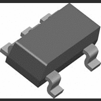
SI9183DT-25-T1 Vishay, SI9183DT-25-T1 Datasheet - Page 10

SI9183DT-25-T1
Manufacturer Part Number
SI9183DT-25-T1
Description
IC, LDO VOLT REG, 2.5V, 150mA, 5-SOT-23
Manufacturer
Vishay
Datasheet
1.SI9183DT-AD-T1-E3.pdf
(11 pages)
Specifications of SI9183DT-25-T1
Primary Input Voltage
6V
Output Voltage Fixed
2.5V
Dropout Voltage Vdo
135mV
No. Of Pins
5
Output Current
150mA
Operating Temperature Range
-40°C To +85°C
Termination Type
SMD
Lead Free Status / RoHS Status
Contains lead / RoHS non-compliant
Available stocks
Company
Part Number
Manufacturer
Quantity
Price
Company:
Part Number:
SI9183DT-25-T1
Manufacturer:
TI
Quantity:
50
Company:
Part Number:
SI9183DT-25-T1-E3
Manufacturer:
Vishay
Quantity:
16 950
Part Number:
SI9183DT-25-T1-E3
Manufacturer:
VISHAY/威世
Quantity:
20 000
Si9183
Vishay Siliconix
DETAILED DESCRIPTION
The Si9183 is a low drop out, low quiescent current, linear
regulator family with very fast transient response. It is primarily
designed for battery powered applications where battery run
time is at a premium. The low quiescent current allows
extended standby time while low drop out voltage enables the
system to fully utilize battery power before recharge. The
Si9183 is a very fast regulator with bandwidth exceeding
50 kHz while maintaining low quiescent current at light load
conditions.
fastest LDO available today. The Si9183 is stable with one of
any output capacitor types from 1 mF to 10.0 mF. However,
X5R or X7R ceramic capacitors are recommended for best
output noise and transient performance.
V
V
is not critical as long as the input supply has low enough source
impedance. For practical circuits, a 1.0-mF or larger ceramic
capacitor is recommended. When the source impedance is
not low enough and/or the source is several inches from the
Si9183, then a larger input bypass capacitor is needed. It is
required that the equivalent impedance (source impedance,
wire, and trace impedance in parallel with input bypass
capacitor impedance) must be smaller than the input
impedance of the Si9183 for stable operation. When the
source impedance, wire, and trace impedance are unknown,
it is recommended that an input bypass capacitor be used of
a value that is equal to or greater than the output capacitor.
V
V
capacitor from V
any value from 1.0 mF to 10.0 mF. A ceramic capacitor with
X5R or X7R dielectric type is recommended for best output
noise, line transient, and load transient performance.
Vishay Siliconix maintains worldwide manufacturing capability. Products may be manufactured at one of several qualified locations. Reliability data for Silicon Technology and
Package Reliability represent a composite of all qualified locations.
http://www.vishay.com/ppg?71258.
www.vishay.com
10
IN
IN
OUT
OUT
is the input supply pin. The bypass capacitor for this pin
is the output voltage of the regulator. Connect a bypass
With this bandwidth, the Si9183 is one of the
OUT
to ground. The output capacitor can be
For related documents such as package/tape drawings, part marking, and reliability data, see
GND
Ground is the common ground connection for V
It is also the local ground connection for C
ADJ
For the adjustable output version, use a resistor divider R1 and
R2, connect R1 from V
R2 should be in the 25-kW to 150-kW range for low power
consumption, while maintaining adequate noise immunity.
The formula below calculates the value of R1, given the
desired output voltage and the R2 value,
SHUTDOWN (SD)
SD controls the turning on and off of the Si9183. V
guaranteed to be on when the SD pin voltage equals or is
greater than 1.2 V. V
pin voltage equals or is less than 0.4 V. During shutdown
mode, the Si9183 will draw less than 1-mA current from the
source. To automatically turn on V
applied, tie the SD pin to V
C
For low noise application, connect a high frequency ceramic
capacitor from C
X7R is recommended.
BP
R1 +
V
ADJ
is nominally 1.215 V.
V
OUT
* V
V
BP
ADJ
ADJ
to ground. A 0.01-mF or a 0.1-mF X5R or
OUT
OUT
R2
is guaranteed to be off when theSD
to ADJ and R2 from ADJ to ground.
IN
.
OUT
S-51147—Rev. G, 20-Jun-05
whenever the input is
Document Number: 71258
BP
, ADJ, and SD.
IN
and V
(1)
OUT
OUT
is
.


