LM35DZ/NOPB National Semiconductor, LM35DZ/NOPB Datasheet - Page 4
LM35DZ/NOPB
Manufacturer Part Number
LM35DZ/NOPB
Description
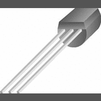
IC, TEMPERATURE SENSOR, ± 0.4°C, TO-92-3
Manufacturer
National Semiconductor
Specifications of LM35DZ/NOPB
Ic Output Type
Voltage
Sensing Accuracy Range
± 0.4°C
Supply Current
91.5µA
Supply Voltage Range
4V To 30V
Sensor Case Style
TO-92
No. Of Pins
3
Msl
MSL 1 - Unlimited
Body Style
TO-92
Brand/series
LM35
Current, Switching
10 mA
Function
Temperature
Mounting Type
PCB
Output
Voltage
Primary Type
Temperature
Range, Measurement
150 °C
Termination
3-Wire Connector
Voltage, Supply
35 V
Voltage, Switching
6 V
Lead Free Status / RoHS Status
Lead free / RoHS Compliant
Lead Free Status / RoHS Status
Lead free / RoHS Compliant
Available stocks
Company
Part Number
Manufacturer
Quantity
Price

Part Number:
LM35DZ/NOPB
Manufacturer:
TI/德州仪器
Quantity:
20 000


Accuracy,
LM35, LM35C
(Note 7)
Accuracy, LM35D
(Note 7)
Nonlinearity
(Note 8)
Sensor Gain
(Average Slope)
Load Regulation
(Note 3) 0 I
Line Regulation
(Note 3)
Quiescent Current
(Note 9)
Change of
Quiescent Current
(Note 3)
Temperature
Coefficient of
Quiescent Current
Minimum Temperature
for Rated Accuracy
Long Term Stability
(Notes 1, 6)
Electrical Characteristics
Note 1: Unless otherwise noted, these specifications apply: −55˚C T
0˚ T
Specifications in boldface apply over the full rated temperature range.
Note 2: Thermal resistance of the TO-46 package is 400˚C/W, junction to ambient, and 24˚C/W junction to case. Thermal resistance of the TO-92 package is
180˚C/W junction to ambient. Thermal resistance of the small outline molded package is 220˚C/W junction to ambient. Thermal resistance of the TO-220 package
is 90˚C/W junction to ambient. For additional thermal resistance information see table in the Applications section.
Note 3: Regulation is measured at constant junction temperature, using pulse testing with a low duty cycle. Changes in output due to heating effects can be
computed by multiplying the internal dissipation by the thermal resistance.
Note 4: Tested Limits are guaranteed and 100% tested in production.
Note 5: Design Limits are guaranteed (but not 100% production tested) over the indicated temperature and supply voltage ranges. These limits are not used to
calculate outgoing quality levels.
Note 6: Specifications in boldface apply over the full rated temperature range.
Note 7: Accuracy is defined as the error between the output voltage and 10mv/˚C times the device’s case temperature, at specified conditions of voltage, current,
and temperature (expressed in ˚C).
Note 8: Nonlinearity is defined as the deviation of the output-voltage-versus-temperature curve from the best-fit straight line, over the device’s rated temperature
range.
Note 9: Quiescent current is defined in the circuit of Figure 1 .
Note 10: Absolute Maximum Ratings indicate limits beyond which damage to the device may occur. DC and AC electrical specifications do not apply when operating
the device beyond its rated operating conditions. See Note 1.
Note 11: Human body model, 100 pF discharged through a 1.5 k
Note 12: See AN-450 “Surface Mounting Methods and Their Effect on Product Reliability” or the section titled “Surface Mount” found in a current National
Semiconductor Linear Data Book for other methods of soldering surface mount devices.
J
Parameter
+100˚C for the LM35D. V
L
1 mA
T
T
T
T
T
T
T
T
T
4V V
V
V
V
4V V
4V V
In circuit of
Figure 1 , I
T
T
T
T
V
S
A
A
A
A
A
A
A
MIN
MIN
A
MIN
A
J
=+5Vdc and I
S
S
S
S
1000 hours
=T
=T
=T
=+25˚C
=−10˚C
=T
=T
=+25˚C
=+25˚C
=+25˚C
=+5V, +25˚C
=+5V
=+30V, +25˚C
=+30V
Conditions
MAX
MIN
S
MAX
MAX
MIN
S
S
T
T
T
A
A
A
30V, +25˚C
30V
30V
, for
T
T
T
L
MAX
MAX
MAX
=0
LOAD
=50 µA, in the circuit of Figure 2 . These specifications also apply from +2˚C to T
Typical
+10.0
±
±
105.5
+0.39
±
±
±
±
±
±
±
±
56.2
+1.5
105
0.2
0.5
0.01
0.02
0.08
56
0.4
0.5
0.8
0.8
0.3
0.4
0.5
resistor.
J
+150˚C for the LM35 and LM35A; −40˚ T
(Note 4)
Tested
+10.2
Limit
+9.8,
LM35
±
±
±
±
2.0
80
82
1.0
1.5
2.0
0.1
(Note 5)
Design
Limit
±
±
±
±
+0.7
+2.0
158
161
3.0
1.5
0.5
5.0
0.2
Typical
±
±
±
+10.0
+0.39
±
±
±
±
±
±
±
±
±
±
56.2
91.5
+1.5
0.2
0.5
0.01
0.02
0.08
56
91
0.4
0.5
0.8
0.8
0.6
0.9
0.9
0.2
0.4
0.5
J
LM35C, LM35D
+110˚C for the LM35C and LM35CA; and
(Note 4)
Tested
Limit
±
±
±
±
2.0
80
82
1.0
1.5
2.0
0.1
MAX
in the circuit of Figure 1 .
(Note 5)
Design
+10.2
Limit
+9.8,
±
±
±
±
±
±
±
±
+0.7
+2.0
138
141
3.0
1.5
1.5
2.0
2.0
2.0
0.5
5.0
0.2
mV/mA
mV/mA
(Max.)
mV/˚C
µA/˚C
Units
mV/V
mV/V
µA
µA
µA
µA
µA
µA
˚C
˚C
˚C
˚C
˚C
˚C
˚C
˚C
˚C
˚C
Related parts for LM35DZ/NOPB
Image
Part Number
Description
Manufacturer
Datasheet
Request
R

Part Number:
Description:
Manufacturer:
National Semiconductor
Datasheet:

Part Number:
Description:
IC, TEMPERATURE SENSOR, ± 0.4°C, TO-92-3
Manufacturer:
National Semiconductor
Datasheet:
Part Number:
Description:
PREC CENTIGRADE TEMP SENSOR
Manufacturer:
National Semiconductor
Part Number:
Description:
PREC CENTIGRADE TEMP SENSOR
Manufacturer:
National Semiconductor
Part Number:
Description:
PREC CENTIGRADE TEMP SENSOR
Manufacturer:
National Semiconductor
Part Number:
Description:
PREC CENTIGRADE TEMP SENSOR
Manufacturer:
National Semiconductor
Part Number:
Description:
PREC CENTIGRADE TEMP SENSOR
Manufacturer:
National Semiconductor
Part Number:
Description:
PREC CENTIGRADE TEMP SENSOR
Manufacturer:
National Semiconductor
Part Number:
Description:
PREC CENTIGRADE TEMP SENSOR
Manufacturer:
National Semiconductor
Part Number:
Description:
PREC CENTIGRADE TEMP SENSOR
Manufacturer:
National Semiconductor
Part Number:
Description:
Temperature Sensor, Precision Fahrenheit Temperature Sensors, Tape and Reel
Manufacturer:
National Semiconductor

Part Number:
Description:
Precision Centigrade Temperature Sensors
Manufacturer:
National Semiconductor

Part Number:
Description:
Precision Centigrade Temperature Sensors
Manufacturer:
National Semiconductor Corporation
Datasheet:
Part Number:
Description:
National Semiconductor [8-Bit D/A Converter]
Manufacturer:
National Semiconductor
Datasheet: